Light emitting apparatus
a technology of light-emitting diodes and light-emitting diodes, which is applied in the direction of electrical apparatus, basic electric elements, and semiconductor devices, can solve the problems of insufficient brightness of micro-light-emitting diodes, and achieve good performan
- Summary
- Abstract
- Description
- Claims
- Application Information
AI Technical Summary
Benefits of technology
Problems solved by technology
Method used
Image
Examples
Embodiment Construction
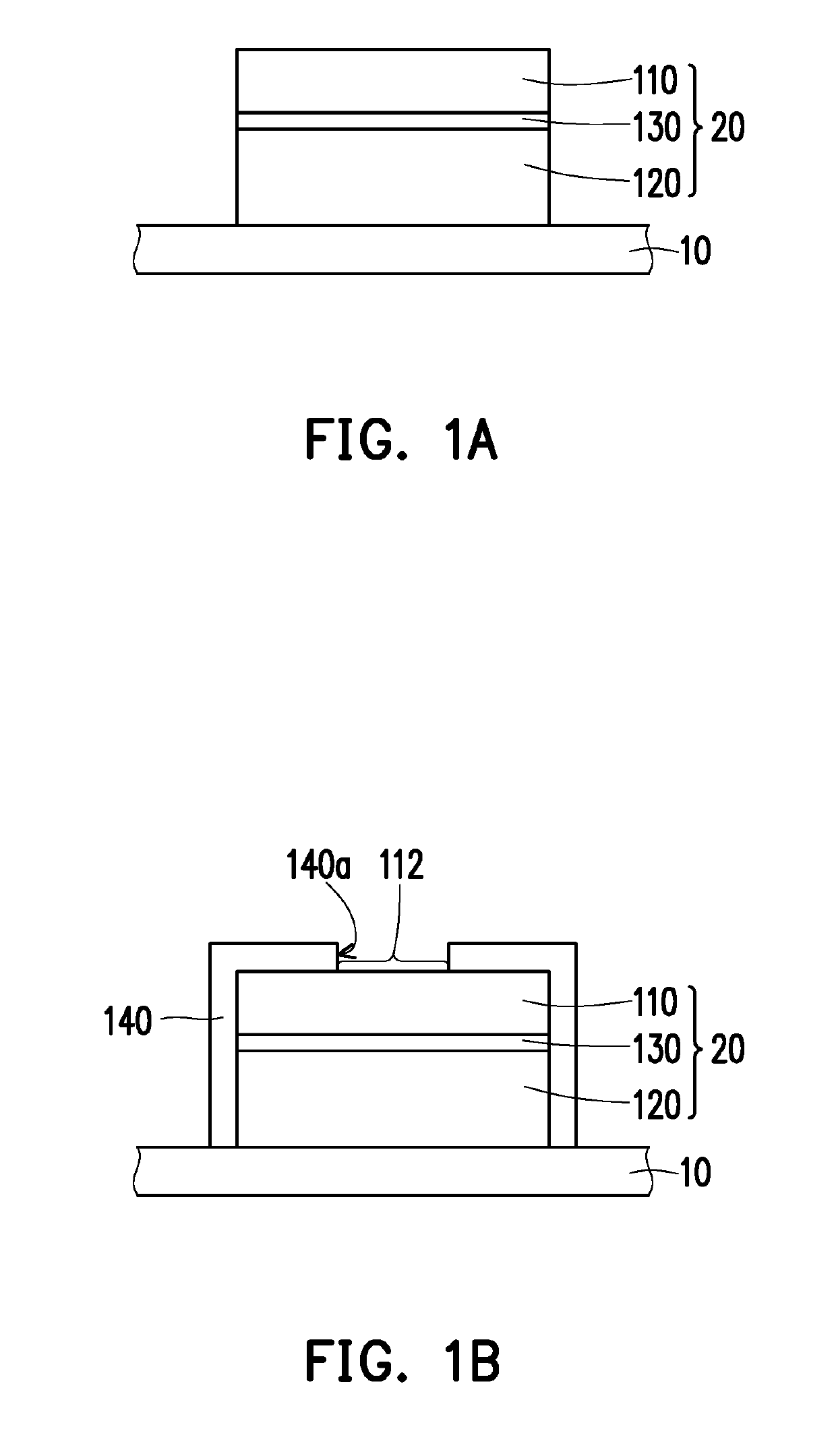
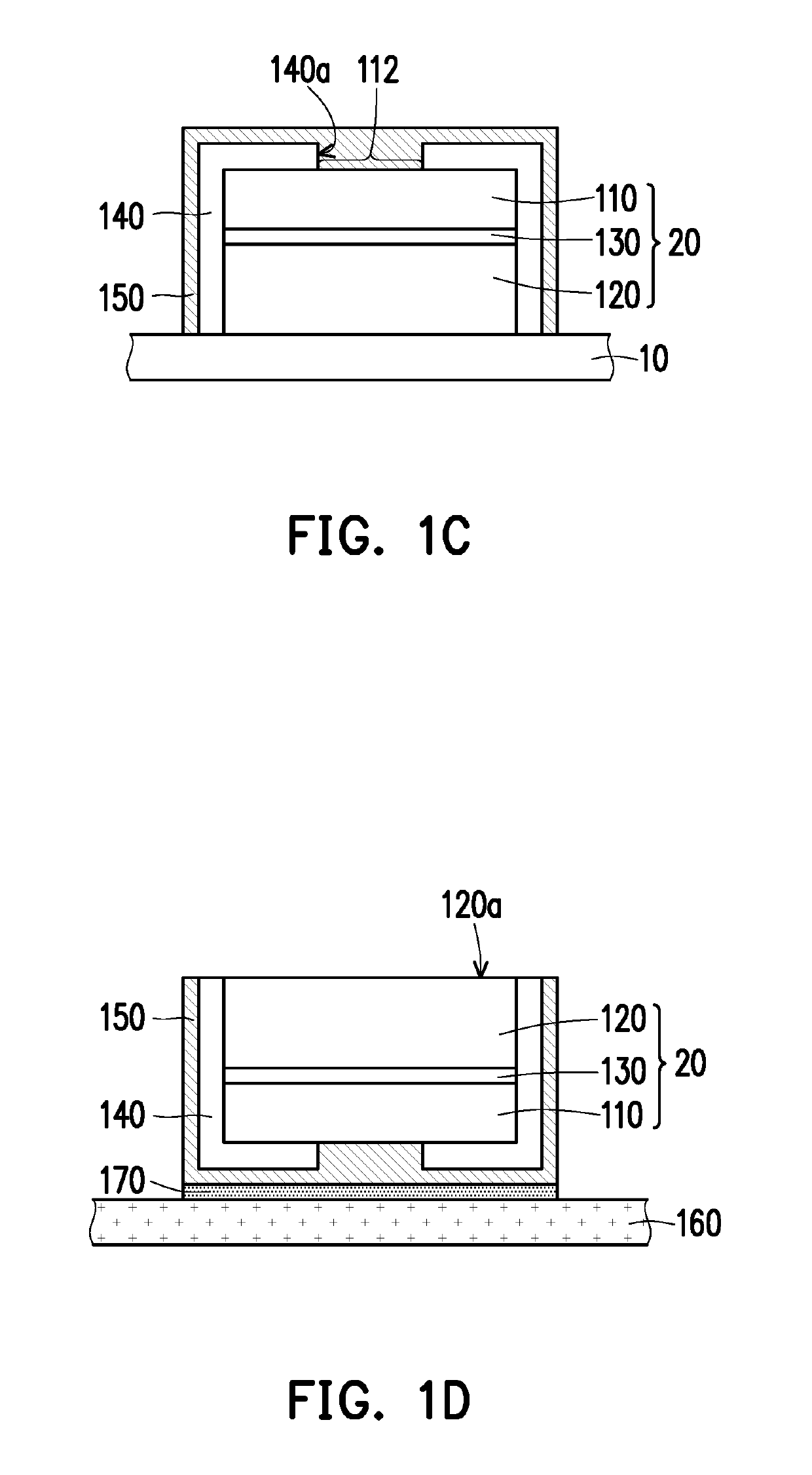
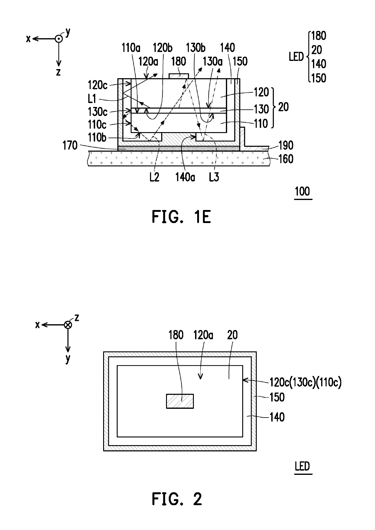
[0015]FIGS. 1A through 1E are schematic cross-sectional views illustrating a process of manufacturing a light emitting apparatus according to an embodiment of the disclosure. Firstly, with reference to FIG. 1A, a growth substrate 10 is provided. In this embodiment, the growth substrate 10 is, for example, a sapphire substrate, but the disclosure is not limited thereto. Then, a semiconductor stacking layer 20 is formed on the growth substrate 10. The semiconductor stacking layer 20 includes a first semiconductor layer 110, a second semiconductor layer 120, and a light emitting layer 130 located between the first semiconductor layer 110 and the second semiconductor layer 120. For example, in this embodiment, the first semiconductor layer 110 includes a P-type semiconductor layer (such as P—GaN), the second semiconductor layer 120 includes an N-type semiconductor layer (such as N—GaN), and the light emitting layer 130 includes a multiple quantum well (MQW) structure. However, the discl...
PUM
 Abstract
Description
Claims
Application Information


