Display device
a technology of a display device and a metal housing, which is applied in the direction of television systems, earth/grounding circuits, pulse automatic control, etc., can solve the problems of limiting the size of the metal housing in the length, width, depth, etc., and reducing the number of grounding sites. , the effect of increasing the complexity of the configuration
- Summary
- Abstract
- Description
- Claims
- Application Information
AI Technical Summary
Benefits of technology
Problems solved by technology
Method used
Image
Examples
first embodiment
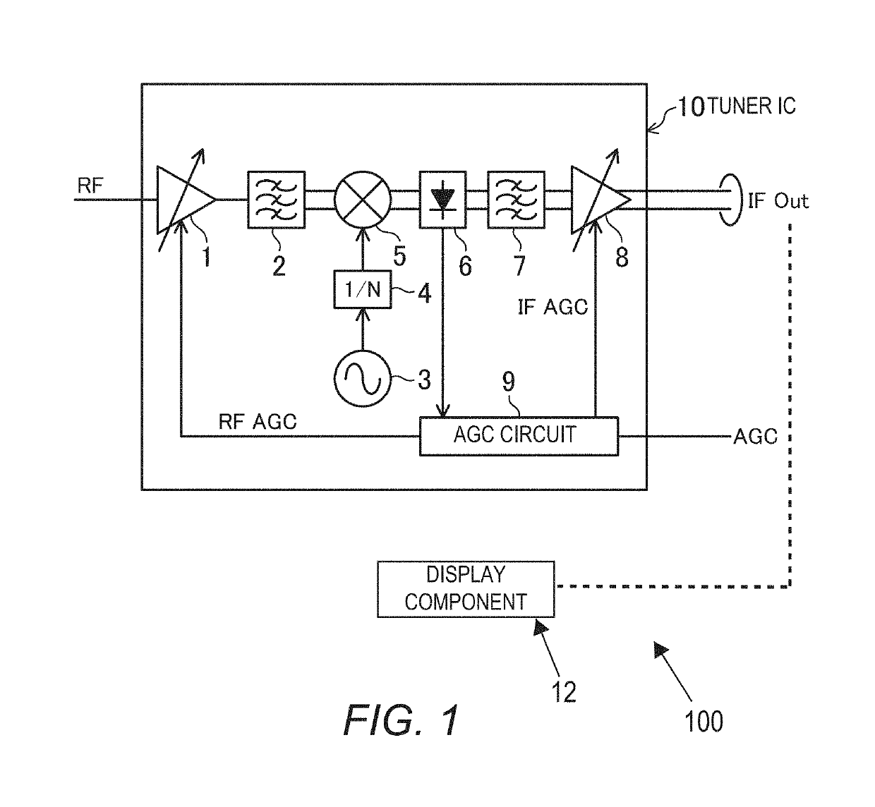
[0060]FIG. 1 is a circuit diagram of a tuner IC provided to a tuner device of a display device 100 pertaining to a first embodiment of the present disclosure. This tuner IC (tuner component) is used for television broadcasts, for example, and its output broadcast signal is outputted to a display component (display) 12, and video corresponding to the broadcast signal is displayed on this display component 12.
[0061]In the tuner IC 10 in FIG. 1, 1 is an RF amplifier (gain control amplifier), 2 is an interstage filter, 3 is a VCO / PLL circuit, 4 is a 1 / N circuit, 5 is a mixer, 6 is a detector, 7 is an interstage filter, 8 is an IF amplifier (gain control amplifier), and 9 is an AGC (auto gain control) circuit.
[0062]The RF amplifier 1 amplifies a received signal having an RF frequency of 90 to 767 MHz, which is the frequency of ground wave television broadcasts in Japan, for example, and the interstage filter 2 limits the band of the amplified signal. The VCO / PLL circuit (oscillator) 3 ch...
first modification example
[0106]FIG. 15 shows a first modification example of the second grounding site shown in FIG. 11.
[0107]In FIG. 11, because the two first grounding sites 22r and 22s are located in point symmetry in a developed view of the housing 22, in this modification example, in FIG. 15, the second grounding site 22w in FIG. 11 is replaced by a second grounding site (second site) 22x that is disposed in point symmetry to the second grounding site 22w, that is, on the bottom edge n of the right face c in a developed view of the housing 22.
[0108]Therefore, again in this modification example, it is possible to lower the impedance in both of the high impedance ranges A and B caused by the two first grounding sites 22r and 22s, with just a single second grounding site 22x.
second modification example
[0109]FIG. 16 shows a second modification example of the position of the second grounding site shown in FIG. 11.
[0110]In this modification example, the configuration in FIG. 12 showing this embodiment is combined with the configuration in FIG. 15 showing the first modification example. The second grounding site 22w in FIG. 12 and the second grounding site 22x in FIG. 15 are disposed as second grounding sites (second sites) that lower the impedance of the two high impedance ranges A and B.
[0111]When the two second grounding sites 22w and 22x are both provided, it will be possible to lower the impedance of the high impedance ranges A and B over a wider range if, for example, one of the grounding sites (such as 22w) is disposed at a position that is separated by a half wavelength (λ / 2) from near a position at the oscillation frequency of 6.8 GHz within the high impedance ranges A and B, and the other grounding site (such as 22x) is disposed at a position that is separated by a half wav...
PUM
 Abstract
Description
Claims
Application Information


