
Integrated circuit structure incorporating stacked field effect transistors and method

a field effect transistor and integrated circuit technology, applied in the direction of transistors, electrical apparatus, semiconductor devices, etc., can solve the problems of limiting the area savings, complex supply of power and/or signal connections to the source/drain region of the lower fets in the stacked pair, and corresponding increase in short channel effects

Active Publication Date: 2019-05-16
GLOBALFOUNDRIES US INC
View PDF0 Cites 26 Cited by
  • Summary
  • Abstract
  • Description
  • Claims
  • Application Information

AI Technical Summary

Benefits of technology

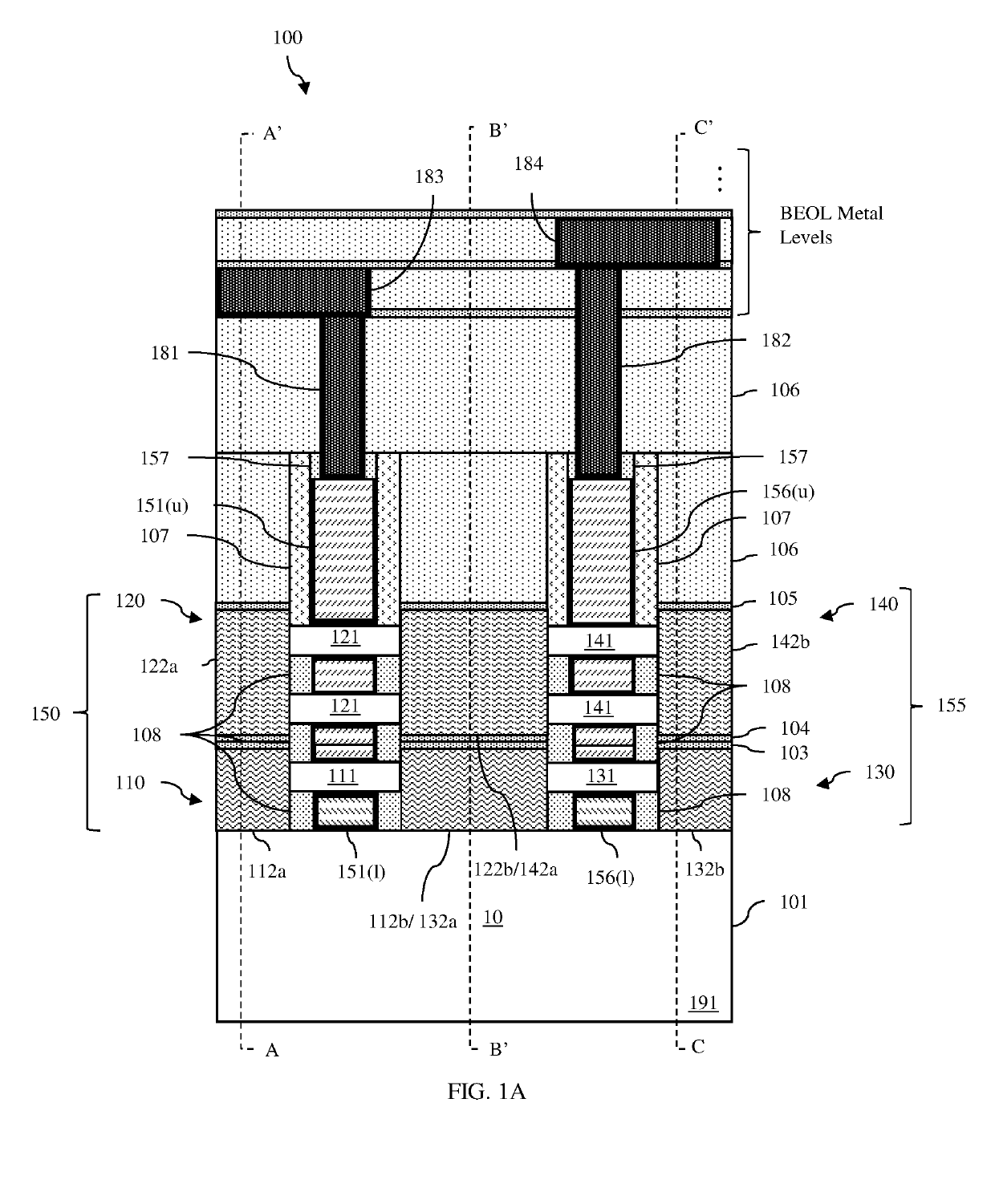
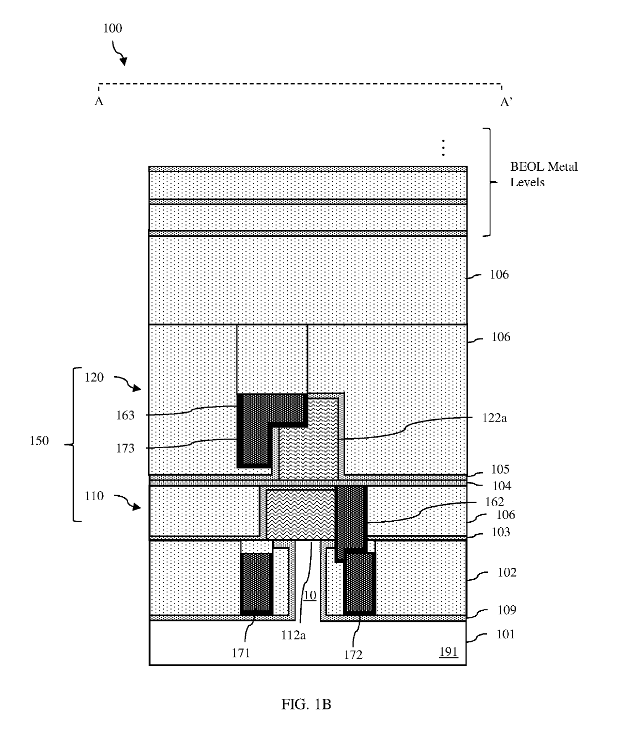
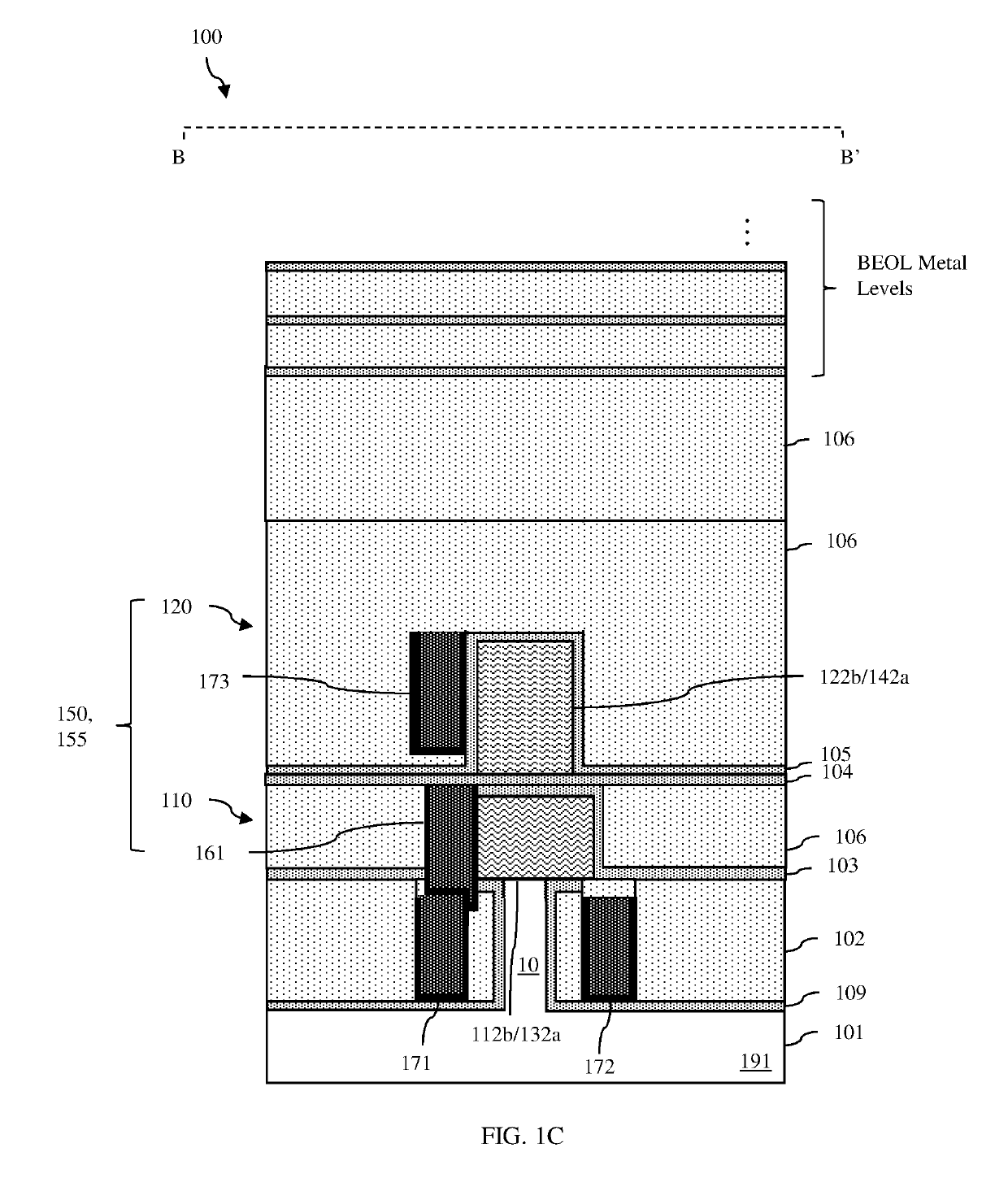
The patent describes an integrated circuit (IC) structure that includes stacked pairs of field effect transistors (FETs) and metal components that enable power and signal connections to the FETs. The structure also includes first and second buried wires, as well as first and second embedded contacts that connect the FETs to the buried wires. The method of forming the structure includes etching a multi-layer fin and forming sidewall spacers on the fin, followed by an etch process to etch a semiconductor substrate to form the semiconductor fin. The first buried wire can be formed at the bottom of a first buried wire trench, and a second embedded contact can be formed at the bottom of a second buried wire trench. The technical effects of this patent include improved power and signal connections, as well as more efficient use of space in the IC structure.

Problems solved by technology

For example, size scaling of planar field effect transistors (FETs) resulted in the development of planar FETs with relatively short channel lengths but, unfortunately, the smaller channel lengths resulted in a corresponding increase in short channel effects.
Unfortunately, while stacked pairs of FETs consume less chip area than side-by-side pairs of FETs, providing the necessary power and / or signal connections to the source / drain regions of the lower FETs in the stacked pairs can be complex and may limit the area savings.

Method used


Image

  • Integrated circuit structure incorporating stacked field effect transistors and method
  • Integrated circuit structure incorporating stacked field effect transistors and method
  • Integrated circuit structure incorporating stacked field effect transistors and method

Examples


Embodiment Construction

[0037]As mentioned above, a conventional layout with multiple field effect transistors (FETs) (e.g., multiple gate-all-around field effect transistors (GAAFETs)) will typically have a row of N-type FETs on one-side, a corresponding row of P-type FETs on the opposite side, and shared gates that traverse and are adjacent to the channel regions of side-by-side pairs of N-type and P-type FETs. Contrarily, a layout with multiple stacked pairs of FETs (e.g., stacked pairs of GAAFETs) will have P-type FETs on one-level, N-type FETs on an adjacent level (i.e., above or below) and, shared gates that extend vertically across and are adjacent to the channel regions of stacked pairs of N-type and P-type FETs. Unfortunately, while stacked pairs of N-type and P-type FETs consume less chip area than side-by-side pairs of N-type and P-type FETs, providing the necessary power and / or signal connections to the source / drain regions of the lower FETs in the stacked pairs can be complex and may limit the...


PUM


Abstract

Disclosed are integrated circuit (IC) structure embodiments that incorporate stacked pair(s) of field effect transistors (FETs) (e.g., gate-all-around FETs), including a lower FET and an upper FET on the lower FET, and various metal components that enable power and / or signal connections to the source / drain regions of those FETs. The metal components can include first buried wire(s) within an isolation region in a level below the stacked pair and a first embedded contact that electrically connects a source / drain region of the lower FET to a first buried wire. Optionally, the metal components can also include second buried wire(s) in dielectric material at the same level as the upper FET and a second embedded contact that electrically connects a source / drain region of the upper FET to a second buried wire. Also disclosed are embodiments of a method of forming such IC structure embodiments.

Description

BACKGROUNDField of the Invention[0001]The present invention relates to integrated circuit (IC) structures and, more particularly, to embodiments of an IC structure that incorporates stacked field effect transistors (FETs), such as stacked gate-all-around field effect transistors (GAAFETs)) and various metal components that enable power and / or signal connections to the source / drain regions of the stacked FETs.Description of Related Art[0002]Integrated circuit (IC) design decisions are often driven by device scalability, device density, manufacturing efficiency and costs. For example, size scaling of planar field effect transistors (FETs) resulted in the development of planar FETs with relatively short channel lengths but, unfortunately, the smaller channel lengths resulted in a corresponding increase in short channel effects.[0003]In response, fin-type FETs (FINFETs) were developed. A FINFET is a non-planar FET that incorporates a semiconductor fin (i.e., an elongated, relatively tal...

Claims


Application Information

Patent Timeline
IPC IPC(8): H01L27/092H01L21/8238H01L29/423H01L29/06H01L29/417
CPCH01L27/0924H01L21/823871H01L29/42372H01L21/823828H01L29/0653H01L21/823878H01L29/41791H01L21/823821H01L21/823807H01L21/8221H01L21/823814H01L27/0688H01L27/092H01L29/66545H01L29/78696H01L29/41733H01L29/42392H01L29/66772H01L29/78654H01L21/823842
Inventor CHANEMOUGAME, DANIELLIEBMANN, LARSXIE, RUILONG
Owner GLOBALFOUNDRIES US INC
Learn More