

Self-aligned contact doping for organic field-effect transistors and method for fabricating the transistor
a field-effect transistor and contact doping technology, applied in the field of self-aligned contact doping for organic field-effect transistors and method for fabricating transistors, can solve the problems of difficult positionally fixed doping, and achieve the effects of increasing electrical conductivity, low cost, and increasing electrical conductivity
- Summary
- Abstract
- Description
- Claims
- Application Information
AI Technical Summary
Benefits of technology
Problems solved by technology
Method used
Image

Examples
Embodiment Construction
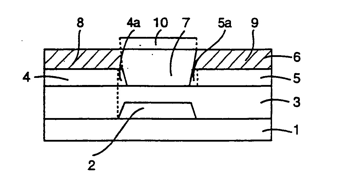
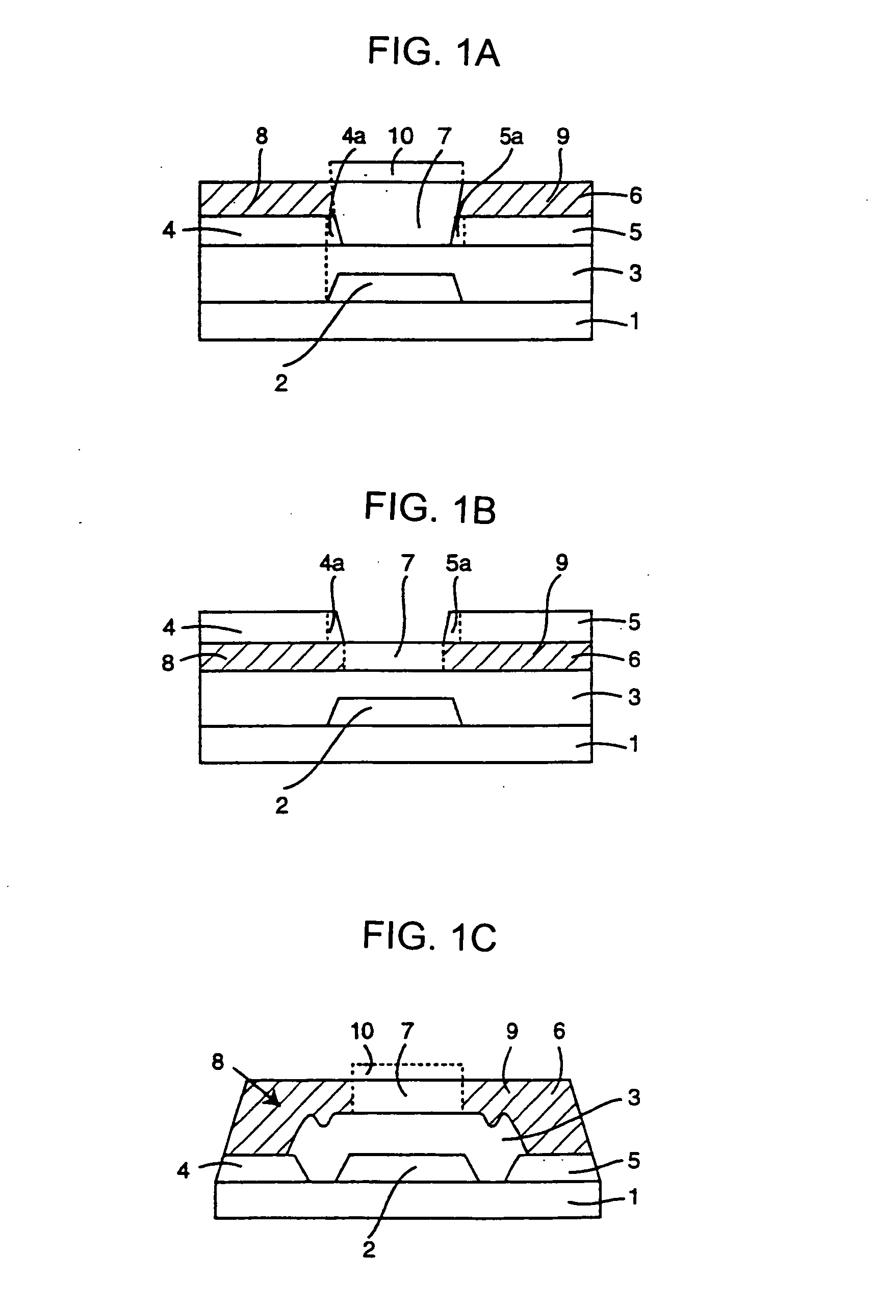
[0062] Referring now to the figures of the drawings in detail and first, particularly to FIGS. 1A, 1B, and 1C thereof, there is shown structures as have, hitherto, been used for organic transistors, these transistors having been modified according to the invention. The structure of the organic transistors that are illustrated in FIG. 1A and 1B requires four deposition and patterning steps, while the structure shown in FIG. 1C requires only three deposition steps.
[0063] For the fabrication of the transistor illustrated in FIG. 1A, first of all, a metal layer is deposited on a substrate 1 and is patterned to obtain the gate electrode 2. The substrate 1 is, for example, of glass or quartz and may also be fabricated from an organic polymer to be able to achieve higher flexibility of the configuration. The gate electrode 2 can be patterned using standard methods, for example, by photolithography, wet-chemical etching, plasma etching, printing, or lifting off. The gate electrode 2 is, th...
PUM
 Abstract
Description
Claims
Application Information