

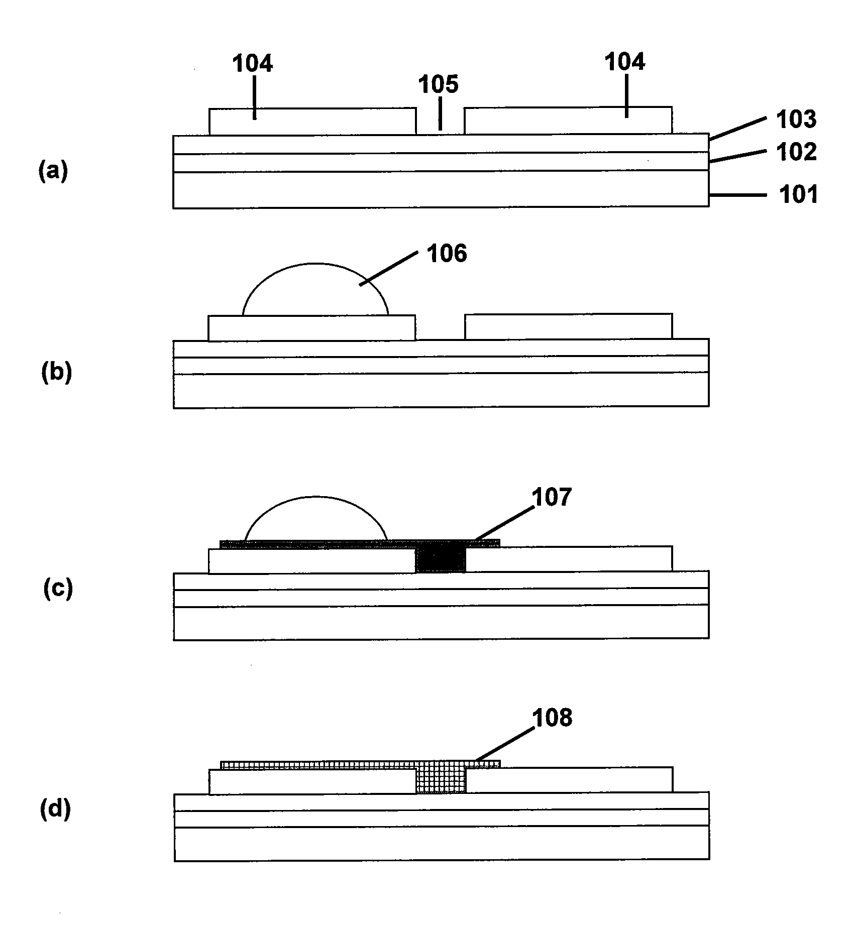
Forming active channel regions using enhanced drop-cast printing
a technology of active channel region and drop-cast printing, which is applied in the direction of electroluminescent light sources, thermoelectric devices, electric lighting sources, etc., can solve the problems of difficult to grow organic single crystals in the highest mobility direction of difficult to grow organic single crystals in active channel region in transistors, and conventional inkjet printing techniques are unable to provide well-oriented organic crystals in active channel regions. , the effect of good electrical properties
- Summary
- Abstract
- Description
- Claims
- Application Information
AI Technical Summary
Benefits of technology
Problems solved by technology
Method used
Image

Examples
first embodiment
[0034]A number of solution-processable organic semiconductor materials have been synthesized, characterized, and fabricated as organic transistors (S. Allard, Angew. Chem. Int. Ed. 2008, 47, 4070).
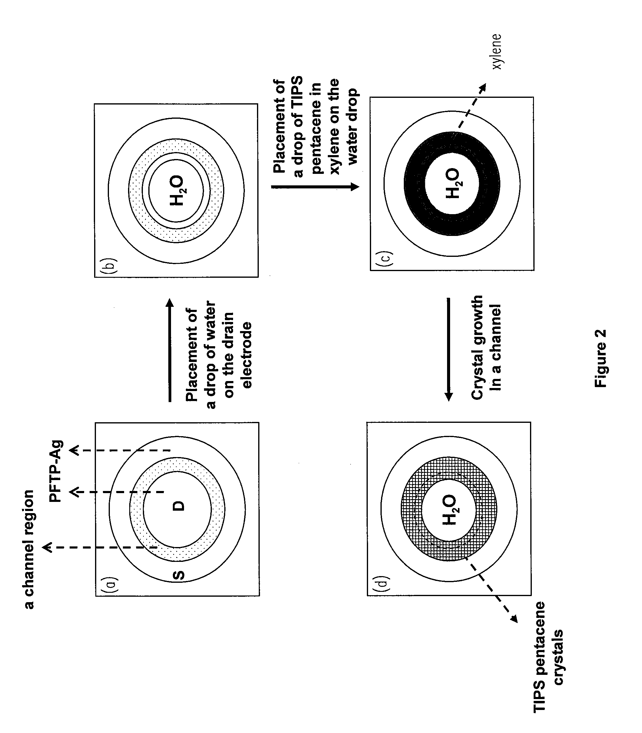
[0035]Among them, a TIPS pentacene has been widely used to fabricate high-performance OTFTs, as it has high solubility in most organic solvents and has a high degree of π-overlap that contribute to the high charge-carrier mobility of OFETs (J. E. Anthony, Angew. Chem. Int. Ed. 2008, 47, 452). In the present exemplary embodiments, to form well-oriented TIPS pentacene crystals on an active channel region in bottom-contact OFETs, the evaporation rates of xylene solvent were appropriately controlled through its interaction with polar H2O.
[0036]FIG. 2 is a schematic illustration of an example of the present method using a two-liquid system. It shows the direct growth of well-oriented TIPS pentacene crystals on an active channel region in bottom-contact OFETs. Dozens of TIPS pentacene crystals a...
second embodiment
[0043]FIG. 7 shows the polarized optical micrograph of the TIPS pentacene transistors fabricated by a conventional drop-casting printing method, whereby bottom-contact electrodes were used and a drop(s) of o-xylene solution (˜0.03 μl) containing TIPS pentacenes (0.8 wt %) was placed onto the top of an active channel region using a micropipette. The conventional drop-casting printing method uses a so-called one-liquid system. The resulting structures were then annealed at around 90° C. for about 10 minutes. In contrast to FIG. 3a, it can be seen that uneven morphology was obtained and thus randomly oriented crystal structures were obtained as a result.
[0044]FIG. 8 shows the transfer characteristics of the two OFETs fabricated by a conventional drop-cast printing method (i.e. a one-liquid system) and the inventive drop-cast printing method (i.e. a so-called two-liquid system). The OFETs fabricated by the inventive drop-cast printing method exhibited better electrical properties, compa...
third embodiment
[0047]FIG. 9 is a polarized optical micrograph of a crystalline TIPS pentacene transistor with square-shaped source and drain electrodes manufactured by the inventive drop-cast method. The third embodiment differs from the first embodiment in the geometric shape of the source and drain electrodes. The TIPS pentacene crystals were grown directly on a square-shaped (or rectangular) active region of the OFETs. The various factors and conditions of the inventive drop-cast procedure or other liquid dropping technique can be modified according to the liquid amount, liquid viscosity, liquid evaporation rates, drop height, drop angle, drop atmosphere, drop splash, etc. Also, the characteristics of the dropping or casting device, such as a pipette system can be adjusted, and the substrate 101 can be processed such that its surface and / or the various layers provided thereon (102, 103, 104) are deposited in an appropriate manner to achieve different configurations such that the desired crystal...
PUM
 Abstract
Description
Claims
Application Information