Organic field effect transistor and method for producing the same

a field effect transistor and organic technology, applied in the direction of transistors, solid-state devices, semiconductor devices, etc., can solve the problems of difficult purification of materials, and improvement of field-effect mobility, so as to achieve high purity, impaired uniformity of film thickness, and reduced mobility

Inactive Publication Date: 2006-04-20
CANON KK
View PDF11 Cites 37 Cited by
  • Summary
  • Abstract
  • Description
  • Claims
  • Application Information

AI Technical Summary

Benefits of technology

[0041] After the light irradiation, the irradiated part precipitates as a fused aromatic ring compound and the non-irradiated part remains as a bicyclic compound. Thus, when the latter part is unnecessary, it is possible to remove it by washing with a solvent. Those solvents which dissolve bicyclic compounds as described above will be selected.
[0042] At the same time as the production of a fused aromatic ring compound by the light irradiation, a crystallized film of the fused aromatic ring compound will be obtained, induced by the crystal growth due to the stacking of aromatic rings. Although the elimination reaction occurs in room temperature, the substrate may be heated to help the crystal growth due to the stacking of aromatic rings. In addition, the crystal growth is also helped by rubbing treatment in which the coating film before light irradiation is lightly rubbed with a cloth or the like. The cloth used for the rubbing treatment includes, but not limited to, rayon, cotton or silk.
[0043] ...

Problems solved by technology

As described above, FET devices using organic semiconductors have required a complicated process such as vacuum deposition or tight control of production conditions (such as temperature and mate...

Method used


Image

  • Organic field effect transistor and method for producing the same
  • Organic field effect transistor and method for producing the same
  • Organic field effect transistor and method for producing the same

Examples


synthesis example 1

Synthesis of Compound (3)

[0072] 5,6,7,8-tetramethylidenebicyclo[2,2,2]oct-2-ene (1) (12 mmol, 1.91 g) and isoamyl nitrite (75 mmol, 10.0 ml) were dissolved in 80 ml of THF (tetrahydrofuran) in a reaction vessel and refluxed by heating. A solution in which anthranilic acid (91 mmol, 12.5 g) was dissolved in 100 ml of THF was charged into a dropping funnel, and it was slowly dropped. After the dropping, heating and stirring were continued until all raw materials are consumed. After the completion of reaction, an aqueous sodium hydroxide solution was added; stirring was continued; and the reaction solution was extracted with hexane. The resultant organic layer was washed with water and saturated saline, dried over anhydrous sodium sulfate and then concentrated to obtain a crude product. This was purified by silica gel column chromatography (hexane) to obtain the compound (3). The yield was 2.66 g (72%).

[0073] Molecular formula: C24H20 (308.42)

[0074] Shape: White crystal

[0075]1H NM...

synthesis example 2

Synthesis of Pentacene (7)

[0110] In a Pyrex (registered trade name) glass cell, 0.005 g of the compound (6) was dissolved in 2 ml of chloroform. The solution was sufficiently degassed and then irradiated with the metal halide lamp at room temperature. Blue crystals were precipitated after several minutes. They were collected by filtration to obtain the objective. Yield 0.004 g (96%).

example 1

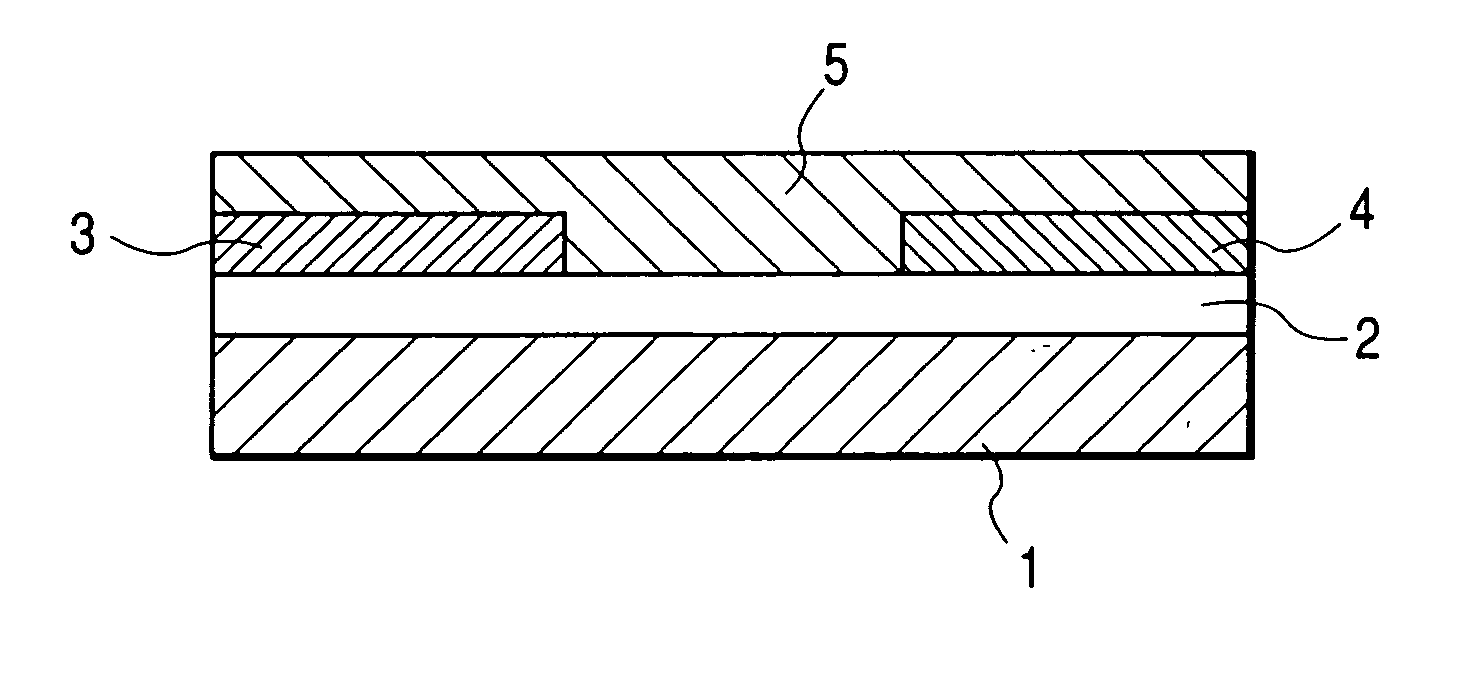
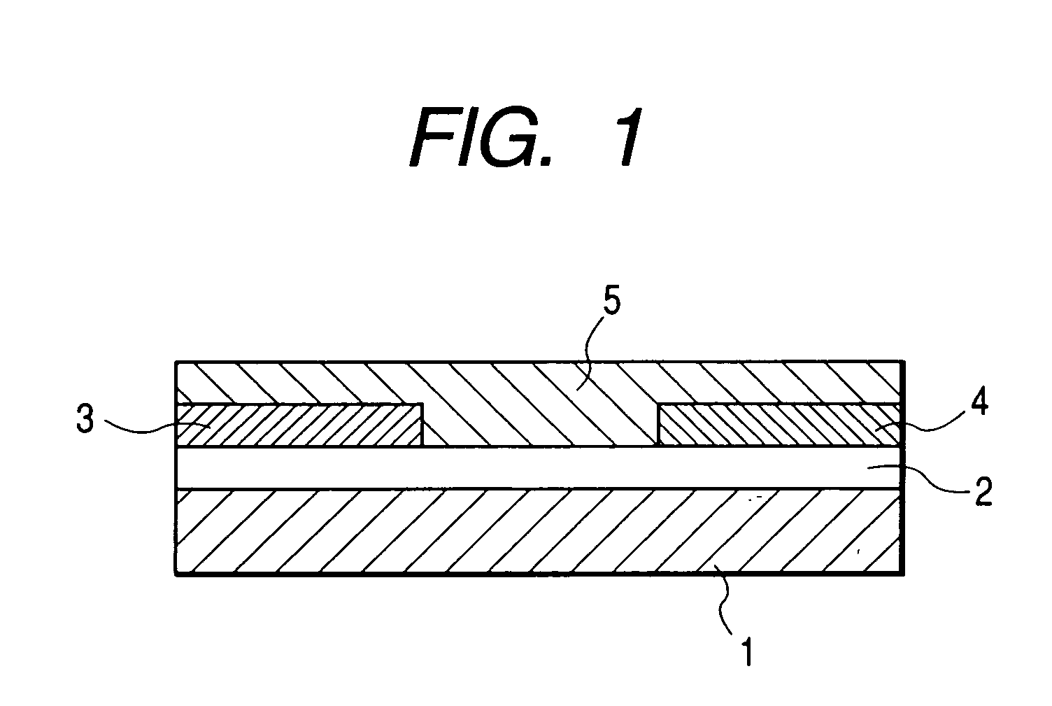
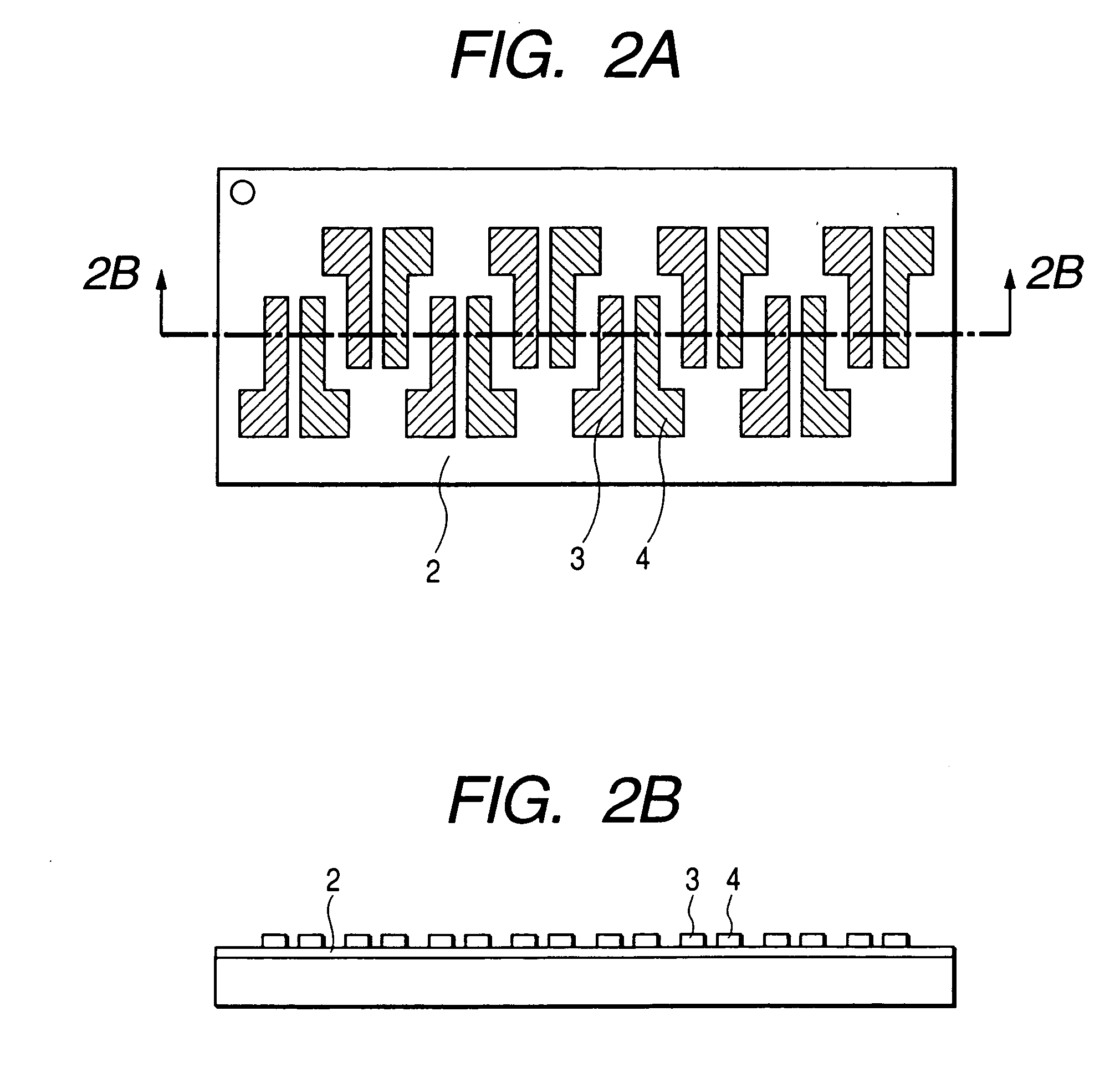
[0111]FIG. 1 shows the structure of the field effect transistor in the present example. First, an N-type silicon substrate was used as a gate electrode 1. A silicon oxide film with a thickness of 500 nm obtained by thermally oxidizing the surface layer of the silicon substrate was used as a gate insulating film 2. Chromium and gold were deposited in mentioned order on the gate insulating film 2, and a source electrode 3 and a drain electrode 4 were formed by a conventional photolithography technique. Then, the resultant substrate was surface-treated by an ozone treatment and then deposited with pentacene (7) prepared in the synthesis example (2) thereon. The film thickness of the thus prepared organic semiconductor layer 5 was 60 nm.

[0112] The field effect transistor with a channel length of 30 μm, a channel width of 10 mm and a thickness of the semiconductor layer of 60 nm was prepared according to the above procedure. The Vd-Id curve of the prepared transistor was measured by Par...


PUM

PropertyMeasurementUnit
Semiconductor propertiesaaaaaaaaaa
Mobilityaaaaaaaaaa

Abstract

There is provided a method for producing a field effect transistor with a high field-effect mobility using a simple method for forming an organic semiconductor layer. A method for producing an organic field effect transistor comprising an organic semiconductor layer, comprising a step of forming the organic semiconductor layer by the photodecomposition of a bicyclic compound containing in a molecule thereof at least one bicyclic ring represented by formula (1):
wherein R1 and R3 each denotes a group for forming an aromatic ring or a heteroaromatic ring which may have a substituent, together with a group to be bonded to R1 or R3; R2 and R4 each denotes a hydrogen atom, an alkyl group, an alkoxy group, an ester group or a phenyl group; and X is a leaving group which denotes carbonyl group or —N═.

Description

TECHNICAL FIELD [0001] The present invention relates to an organic field effect transistor and a method for producing the same, and specifically to a field effect transistor with a high mobility using a fused aromatic ring compound obtained by irradiating a fused aromatic ring compound precursor that is soluble in a solvent with light as an organic semiconductor layer. Further, the present invention relates to a method for producing a field effect transistor in which a field effect transistor with a high mobility can be easily produced by using a film of a fused aromatic ring compound obtained by irradiating a coating film of a fused aromatic ring compound precursor that is soluble in a solvent with light as an organic semiconductor layer. BACKGROUND ART [0002] Non-linear optical properties, electrical conductivity and semiconductivity of organic semiconductor compounds have received attention in the organic electronics and optoelectronics fields and the development of various devic...

Claims


Application Information

Patent Timeline
IPC IPC(8): H01L31/109H01L21/336H01L29/786H01L51/05H01L51/00H01L51/30H01L51/40
CPCH01L51/0003H01L51/0044H01L51/0052H01L51/0055H01L51/0056H01L51/0545H10K71/12H10K85/154H10K85/623H10K85/624H10K85/615H10K10/466
Inventor MIYAZAKI, HAJIMEMIURA, DAISUKENAKAYAMA, TOMONARIUNO, HIDEMITSUONO, NOBORU
Owner CANON KK
Why Eureka
Try Eureka