Method for structuring an OFET

a technology of organic field effect transistor and structure method, which is applied in the direction of transistors, solid-state devices, thermoelectric devices, etc., can solve the problems of difficult structure of ofets, inability to structure in this way, and substantial reduction of ofet performance, etc., to achieve the effect of high resolution, cost-effective, and compact structur

Inactive Publication Date: 2005-11-01
POLYIC
View PDF124 Cites 37 Cited by
  • Summary
  • Abstract
  • Description
  • Claims
  • Application Information

AI Technical Summary

Benefits of technology

[0006]It was therefore an object of the invention to provide a cost-effective method for structuring OFETs with high resolution which is suitable for mass-production. Furthermore, it is an object of the invention to provide an OFET which is more powerful, because it is equipped with more structured layers, and which is more compact and can be produced with a smaller distance l.

Problems solved by technology

A different conductive organic material, e.g. polypyrrole, cannot readily be structured in this way.
The lack of structuring of the other layers, such as at least the structuring of semiconducting and of the insulating layer comprising functional polymers (which may be present in polymeric or oligomeric form), leads to a substantial reduction in performance of the OFETs obtained, but it is dispensed with for cost reasons.
However, lengths l of less than 10 μm are desirable, and hence at present no structuring method apart from the complicated lithography method appears reasonable.

Method used


Image

  • Method for structuring an OFET
  • Method for structuring an OFET
  • Method for structuring an OFET

Examples


Embodiment Construction

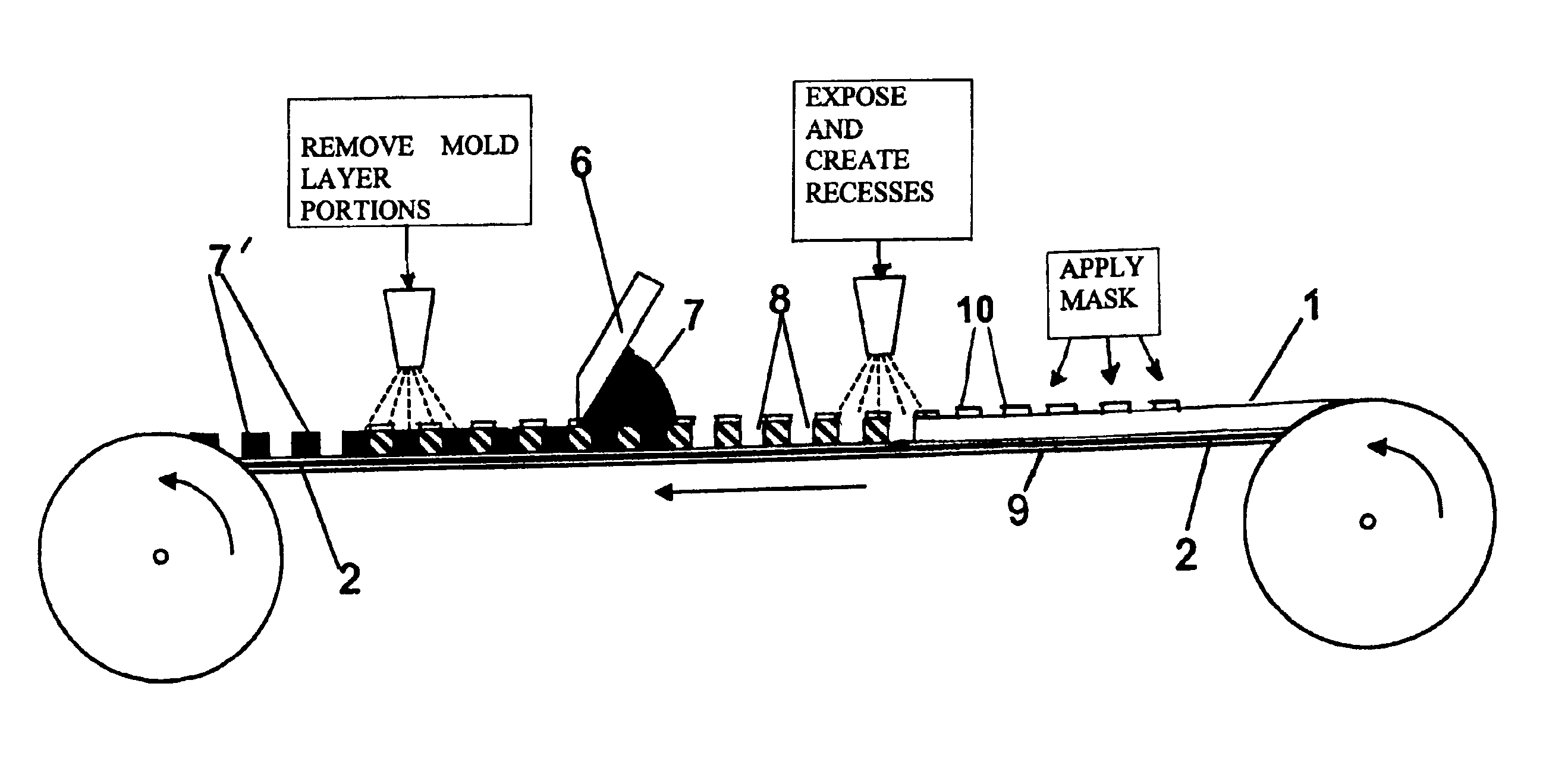
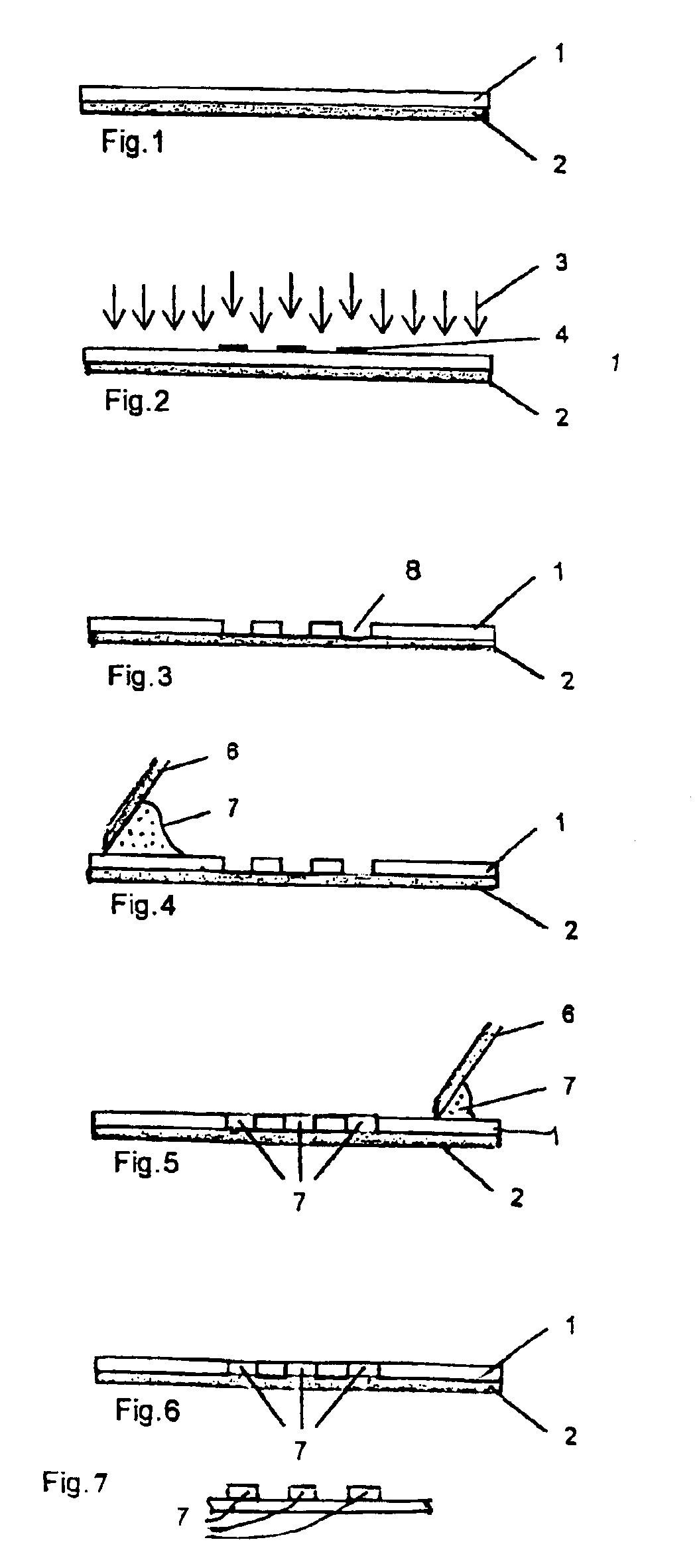
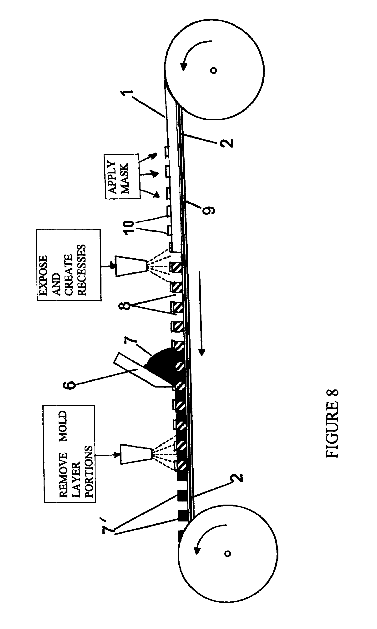
[0021]The method comprises the following operations:[0022]a) an optionally whole-area mold layer, which need not be restricted to the region which is to be structured, is applied to a substrate or a lower layer; this mold layer is not the functional polymer (i.e. semiconducting, conductive or insulating layer) but another organic material which serves as a mold or block for the conductive organic electrode layer; this other organic material should have insulating properties;[0023]b) by exposure through a mask, the mold layer acquires recesses which correspond to the structures;[0024]c) the functional polymer is then scraped in liquid form, as a solution and / or as a melt into these recesses.

[0025]The negative mold of the structure on the mold layer can be produced by exposing a photoresist layer on the substrate or a lower layer. The material of the negative mold may be a photoresist which has recesses after exposure through a mask, such as, for example, a shadow mask, or another str...


PUM


Abstract

The invention relates to an organic field effect transistor, a method for structuring an OFET and an integrated circuit with improved structuring of the functional polymer layers. Structuring is achieved by scraping the functional polymer into a mold layer in which recesses are initially produced by exposure.

Description

CROSS REFERENCE TO RELATED APPLICATIONS[0001]This is the 35 USC 371 national stage application PCT / DE01 / 03318 filed on Aug. 29, 2002, which designated the United States of America.FIELD OF THE INVENTION[0002]The invention relates to an organic field effect transistor, a method for structuring an OFET and an integrated circuit with improved structuring of the functional polymer layers.BACKGROUND OF THE INVENTION[0003]Integrated plastic circuits based on OFETs are used for microelectronic mass applications and disposable products such as identification and product tags. A tag is, for example, an electronic bar code of the kind provided on merchandise or on luggage. OFETs have a wide range of uses as RFID tags: radio frequency identification tags, which need not be arranged only on the surface. In the case of OFETs for these applications, the excellent operating behavior of silicon technology can be dispensed with, but by the same token low production costs and mechanical flexibility s...

Claims


Application Information

Patent Timeline
Patent Type & Authority Patents(United States)
IPC IPC(8): H01L51/40H01L51/05H01L21/336H01L29/786H01L35/24H01L51/10
CPCH01L51/0004H01L51/0508H10K71/13H10K10/46
Inventor BERNDS, ADOLFCLEMENS, WOLFGANGFIX, WALTERROST, HENNING
Owner POLYIC
Why Eureka
Try Eureka