Semiconductor Structure and Method for Manufacturing the Same

a technology of semiconductors and semiconductors, applied in the direction of semiconductor devices, electrical devices, transistors, etc., can solve the problems of short channel effects, and achieve the effects of reducing parasitic capacitance, parasitic capacitance reduction, and contact resistance reduction of the source extension region

Inactive Publication Date: 2012-09-20
INST OF MICROELECTRONICS CHINESE ACAD OF SCI
View PDF12 Cites 50 Cited by
  • Summary
  • Abstract
  • Description
  • Claims
  • Application Information

AI Technical Summary

Benefits of technology

[0026]By removing at least a part of the source-side portion of the spacer, the thickness of the source-side portion is less than that of the drain-side portion. The formation of the contact layer on portions of the active region exposed by the spacer and the gate stack or dummy gate stack makes the contact layer at the source side closer to the gate stack than that at the drain side. Compared with the semiconductor structure with the same thickness of the source-side portion, the distance between the contact layer at the drain side and the gate stack is larger, which is beneficial to the reduction of the parasitic capacitance between the drain extension region and the gate; compared with the semiconductor structure with the same thickness of the drain-side portion, the distance between the contact layer at the source side and the gate stack is smaller, which is beneficial to the reduction of the contact resistance of the source extension region.
[0027]By forming the first contact layer on the upper surface of the active region at the source side, and then etching the interlayer dielectric layer to form a contact hole (conductive metal is filled in the contact hole to form the contact plug) after the formation of the interlayer dielectric layer, the contact hole at least exposes a part of a portion of the active region at the drain side. The formation of the second contact layer on part of the active region makes the first contact layer closer to the gate stack than the second contact layer under the precondition that the thicknesses of the source-side portion and the drain-side portion are the same, so as to possibly make the distance between the second contact layer and the gate stack larger, which is beneficial to the reduction of the parasitic capacitance between the drain extension region and the gate.
[0028]Further, by symmetrically removing at least one part of the spacer, the distance between the first contact layer and the gate stack is smaller, which is beneficial to the reduction of the contact resistance.

Problems solved by technology

With continuous reduction in a size of the semiconductor structure, a length of a channel beneath a gate decreases correspondingly, thereby causing occurrence of short channel effects.
Therefore, it is a problem urgently to be solved to strike a balance between the reduction in the contact resistance of the source extension region and that in the parasitic capacitance between the gate and the drain extension region in the semiconductor structure.

Method used


Image

  • Semiconductor Structure and Method for Manufacturing the Same
  • Semiconductor Structure and Method for Manufacturing the Same
  • Semiconductor Structure and Method for Manufacturing the Same

Examples


Embodiment Construction

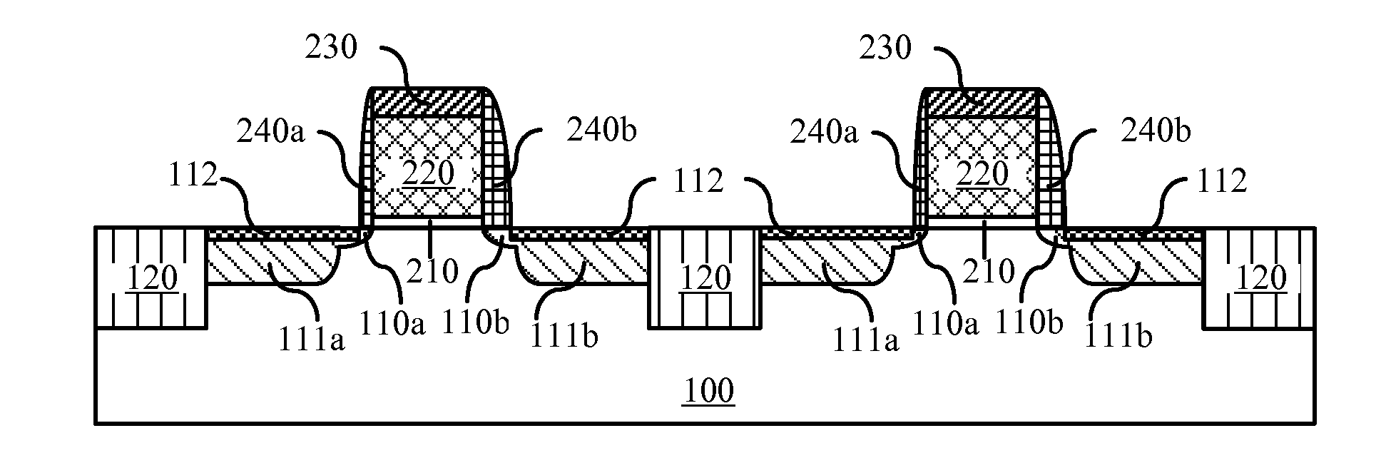
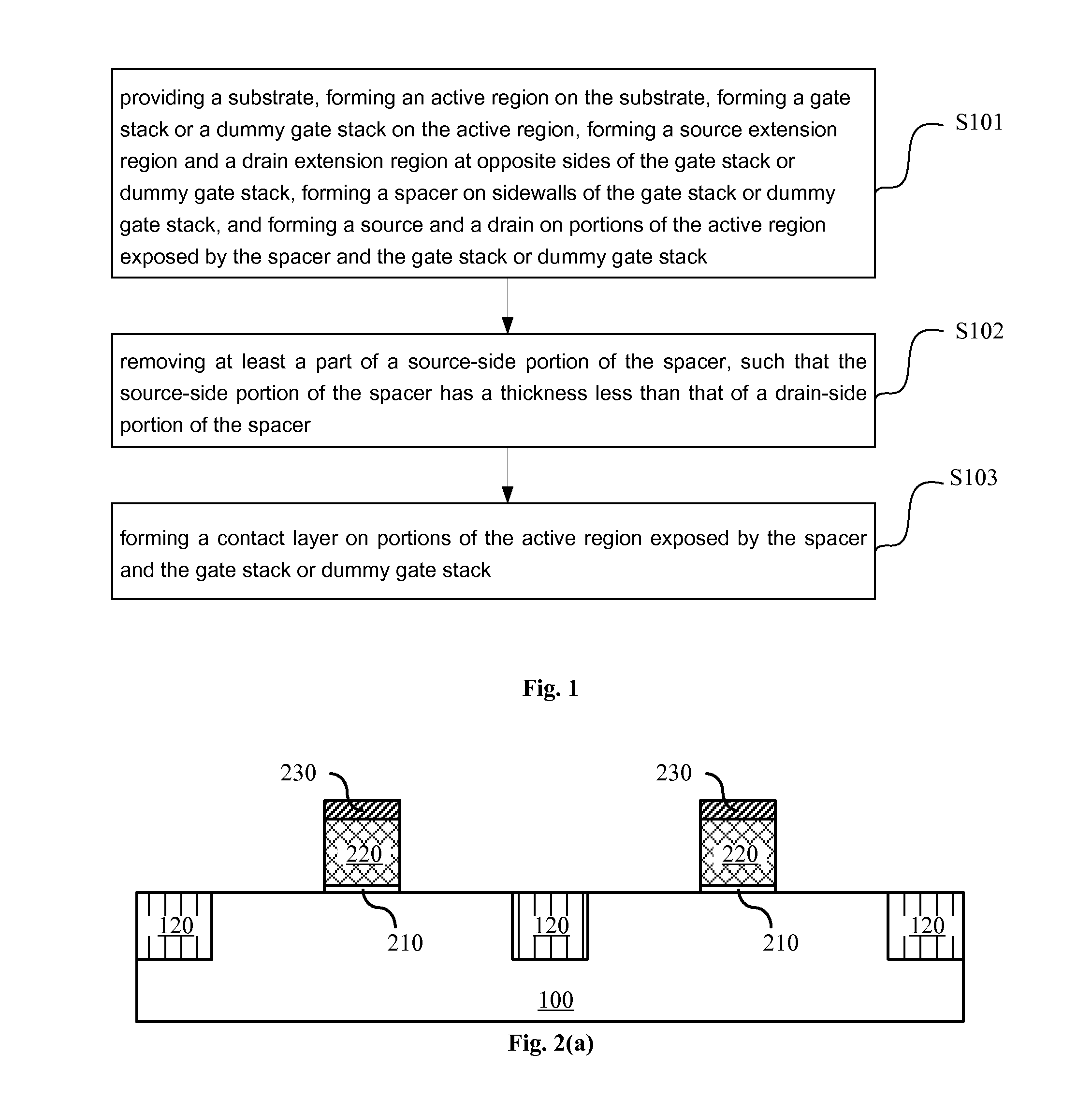
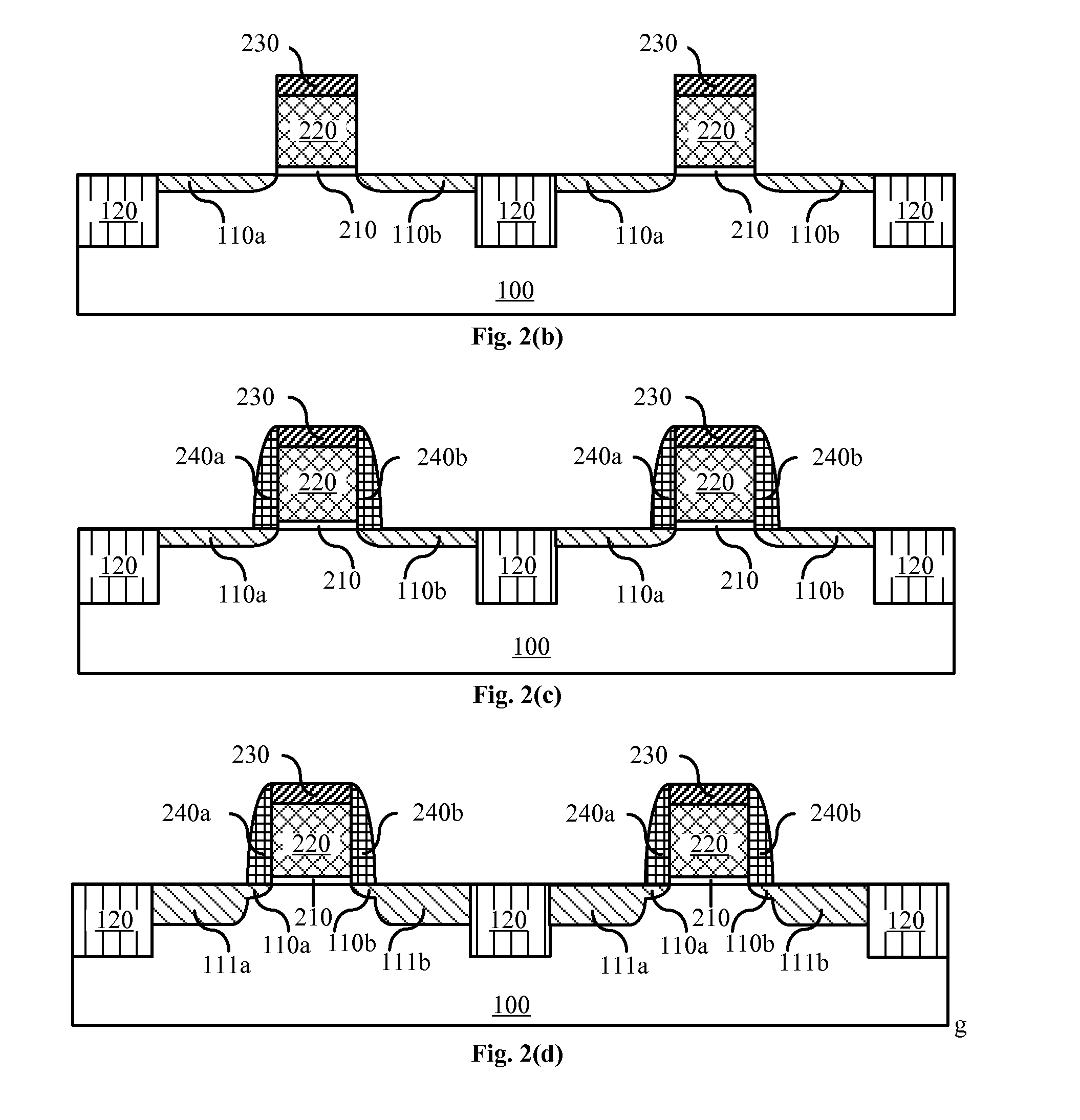
[0036]The embodiments of the present invention are described in detail as follows, the examples of which are shown in the drawings. The embodiments described as follows in reference to the drawings are exemplary and merely used to interpret the present invention, instead of restricting the present invention.

[0037]The following disclosure provides many different embodiments or examples for implementing different structures of the present invention. In order to simplify the disclosure of the present invention, the components and arrangement of specific examples are described in the following text. Apparently, they are just exemplary, and do not intend to restrict the present invention. In addition, reference numbers and / or letters can be repeatedly used in different examples of the present invention for the purposes of simplification and clearness, without indicating the relationships between the discussed embodiments and / or arrangements. Furthermore, the present invention provides ex...


PUM


Abstract

A method for manufacturing a semiconductor structure comprises: providing a substrate, forming an active region on the substrate, forming a gate stack or a dummy gate stack on the active region, forming a source extension region and a drain extension region at opposite sides of the gate stack or dummy gate stack, forming a spacer on sidewalls of the gate stack or dummy gate stack, and forming a source and a drain on portions of the active region exposed by the spacer and the gate stack or dummy gate stack; removing at least a part of a source-side portion of the spacer, such that the source-side portion of the spacer has a thickness less than that of a drain-side portion of the spacer; and forming a contact layer on portions of the active region exposed by the spacer and the gate stack or dummy gate stack. Correspondingly, the present invention further provides a semiconductor structure. The present invention is beneficial to the reduction of the contact resistance of the source extension region and meanwhile can also reduce the parasitic capacitance between the gate and the drain extension region.

Description

[0001]This application claims priority to a Chinese Patent Application No. 201110066929.0, filed on Mar. 18, 2011 and entitled “SEMICONDUCTOR STRUCTURE AND METHOD FOR MANUFACTURING THE SAME”, which is hereby incorporated by reference in its entirety.FIELD OF THE INVENTION[0002]The present invention relates to the semiconductor manufacturing technology, and particularly to a semiconductor structure and a method for manufacturing the same.BACKGROUND OF THE INVENTION[0003]A metal-oxide-semiconductor field-effect transistor (MOSFET) is a transistor that can be widely used in digital circuits and analog circuits. With continuous reduction in a size of the semiconductor structure, a length of a channel beneath a gate decreases correspondingly, thereby causing occurrence of short channel effects. A common means for reducing short channel effects is to form a source extension region and a drain extension region with a shallow depth.[0004]In order to improve the performance of the semiconduc...

Claims


Application Information

Patent Timeline
Patent Type & Authority Applications(United States)
IPC IPC(8): H01L27/088H01L29/772H01L21/336
CPCH01L21/823807H01L21/823814H01L21/823864H01L29/41775H01L29/456H01L29/4966H01L21/28518H01L29/665H01L29/6653H01L29/66545H01L29/6659H01L29/7835H01L21/26586H01L29/517
Inventor YIN, HAIZHOULUO, ZHIJIONGZHU, HUILONG
Owner INST OF MICROELECTRONICS CHINESE ACAD OF SCI
Why Eureka
Try Eureka