

Power amplifier module
- Summary
- Abstract
- Description
- Claims
- Application Information
AI Technical Summary
Benefits of technology
Problems solved by technology
Method used
Image

Examples
first embodiment
(1) Configuration of RF Signal Processing Module 100
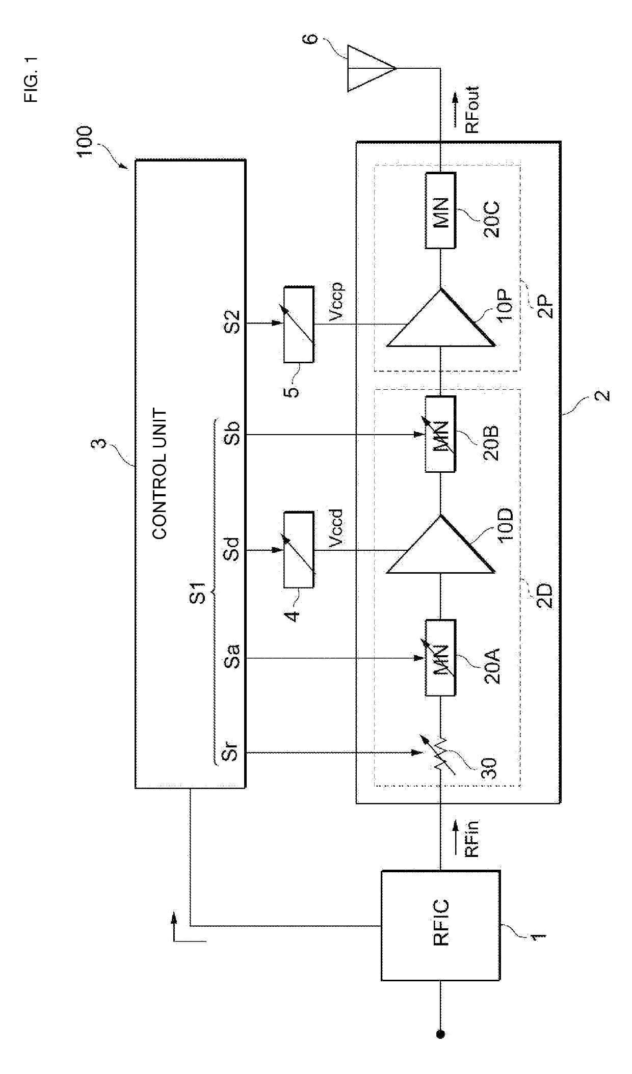
[0018]FIG. 1 is a circuit diagram of a radio frequency (RF) signal processing module 100 according to a first embodiment of the present disclosure. The RF signal processing module 100 includes a radio frequency integrated circuit (RFIC) 1, a power amplifier module 2, a control unit 3 (e.g., a control circuit such as a controller, microprocessor, integrated circuit, or the like), a power supply circuit 4, and a power supply circuit 5.
(1-1) RFIC 1
[0019]The RFIC 1 is a radio frequency integrated circuit, and modulates a signal supplied from a baseband processing unit or the like, which is not illustrated, into a high-frequency signal to generate a radio frequency (RF) signal. The frequency of an RF signal ranges from about several hundred MHz to several GHz, for example.
(1-2) Power Amplifier Module 2
[0020]The power amplifier module 2 is a circuit that amplifies an RF signal generated by the RFIC 1. As illustrated in FIG. 1, the power ...
second embodiment
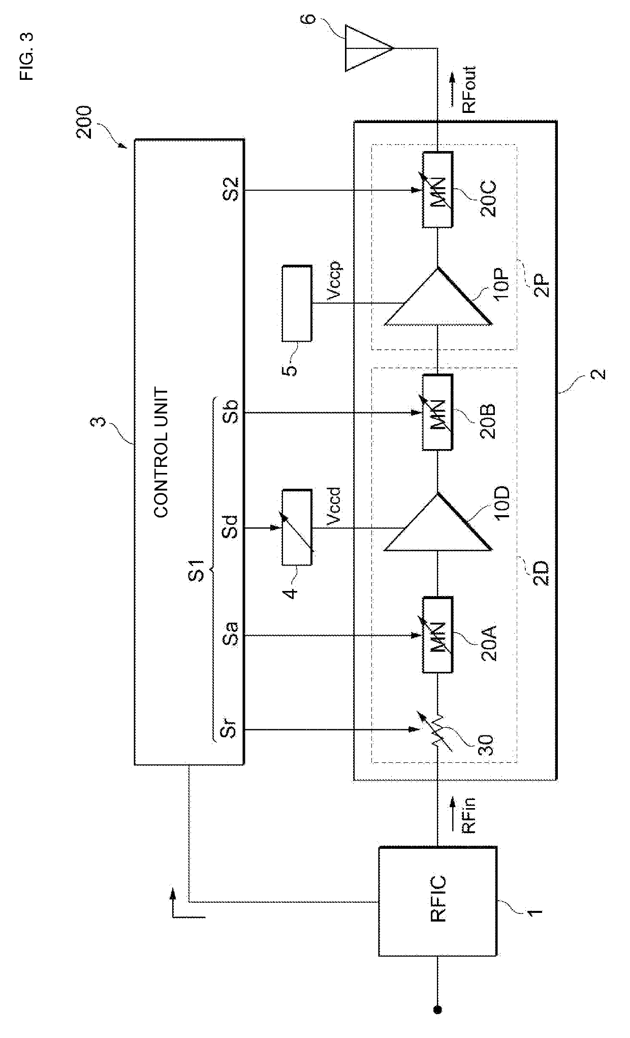
[0040]FIG. 3 is a circuit diagram of an RF signal processing module 200 according to a second embodiment of the present disclosure. Hereinafter, among elements of the RF signal processing module 200, elements that differ from those of the RF signal processing module 100 according to the first embodiment of the present disclosure will be described, and the description of elements that are the same as those of the RF signal processing module 100 is appropriately omitted.
(1) Configuration of RF Signal Processing Module 200
[0041]As described below, the impedance of the matching network 20C included in the RF signal processing module 200 is variable. The control unit 3 included in the RF signal processing module 200 generates, as the second control signal S2, a control signal for controlling the matching network 20C.
[0042]The matching network 20C included in the RF signal processing module 200 is, for example, a low pass filter circuit having variable impedence as illustrated in FIG. 4A....
PUM
 Abstract
Description
Claims
Application Information