Litho-litho-etch double patterning method

a technology of litholithoetch and double patterning, applied in the field of double patterning methods, can solve the problems of inability to create sadp or saqp, the metal level of dram and logic chips is more complex, and the cost of lele can be high

Active Publication Date: 2019-05-30
GLOBALFOUNDRIES US INC
View PDF1 Cites 0 Cited by
  • Summary
  • Abstract
  • Description
  • Claims
  • Application Information

AI Technical Summary

Benefits of technology

[0006]Double patterning methods for use in the process of producing a semiconductor device such as an integrated circuit are disclosed. In a first aspect of the disclosure, a double patterning method includes: forming a sole resist layer by coating a substrate with a resist composition wherein solubility of the resist composition in a positive developer increases upon irradiation with ultraviolet (UV) rays of a first radiant energy density and solubility of the resist composition in a negative developer decreases upon irradiation with UV rays of a second radiant energy density, the second radiant energy density of UV rays being greater than the first radiant energy density of UV rays; exposing the resist layer to the first radiant energy density of UV rays; forming a first pattern in the resist layer by developing the resist layer with the positive developer; exposing the resist layer to the second radiant energy density of UV rays; and forming a second pattern in the resist layer by developing the resist layer with the negative developer, the second pattern including one or more features of the first pattern.
[0007]In a second aspect of the disclosure, a double patterning method includes: forming a resist layer by coating a substrate with a resist composition wherein solubility of the resist composition in a positive developer increases upon irradiation with ultraviolet (UV) rays of a first radiant energy density and solubility of the resist composition in a negative developer decreases upon irradiation with UV rays of a second radiant energy density, the second radiant energy density of

Problems solved by technology

LELE typically provides a 30% reduction in pitch, but LELE can be expensive, as it doubles the process steps in the lithography flow.
Metal levels in DRAM and logic ch

Method used


Image

  • Litho-litho-etch double patterning method
  • Litho-litho-etch double patterning method
  • Litho-litho-etch double patterning method

Examples


Embodiment Construction

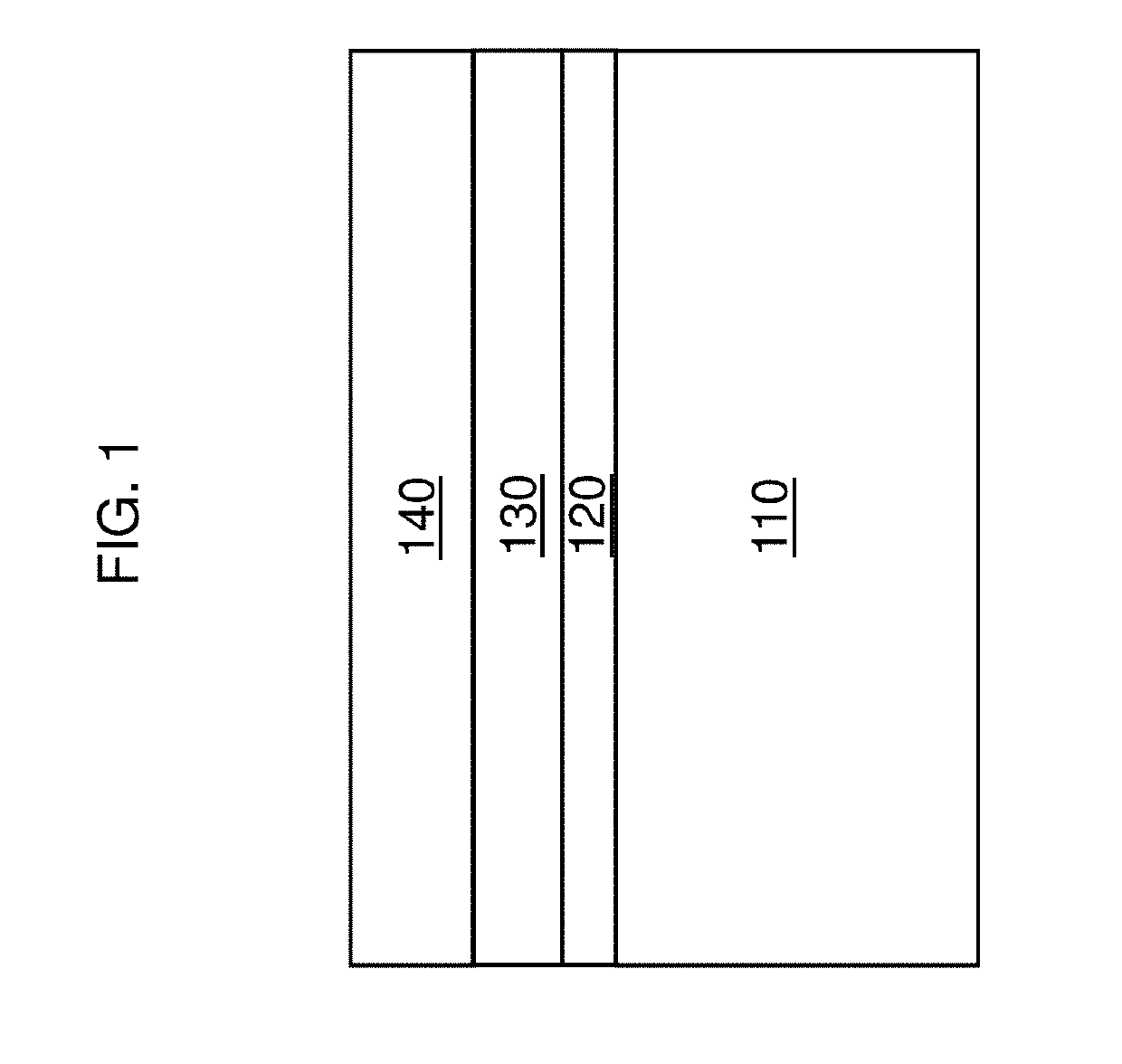
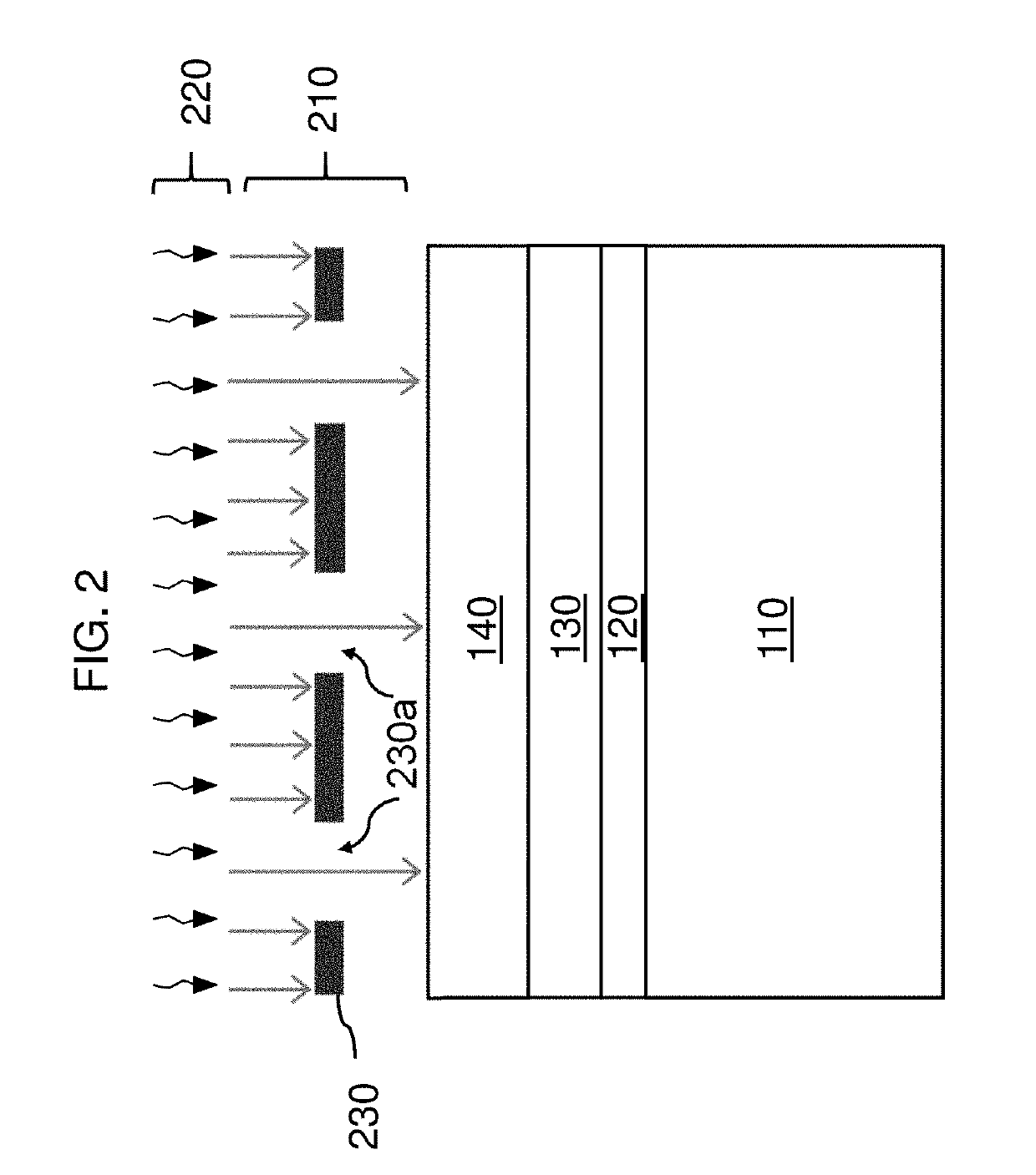
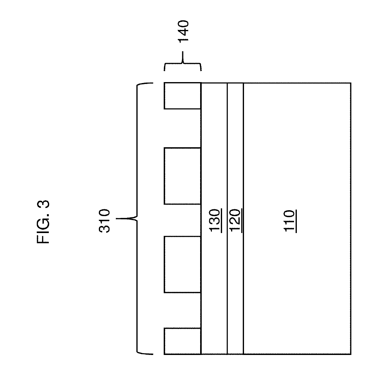
[0019]Detailed embodiments of the claimed structures and methods are disclosed herein; however, it can be understood that the disclosed embodiments are merely illustrative of the claimed structures and methods that may be embodied in various forms. The subject matter of this disclosure may, however, be embodied in many different forms and should not be construed as limited to the exemplary embodiments set forth herein. Rather, these exemplary embodiments are provided so that this disclosure will be thorough and complete and will fully convey the scope of this disclosure to those skilled in the art.

[0020]In the interest of not obscuring the presentation of embodiments of the present disclosure, in the following detailed description, some processing steps or operations that are known in the art may have been combined together for presentation and for illustration purposes and in some instances, may have not been described in detail. In other instances, some processing steps or operati...


PUM


Abstract

A litho-litho-etch double patterning method including forming a resist layer by coating a substrate with a resist composition; exposing the resist layer to a first radiant energy density of UV rays; forming a first pattern in the resist layer by developing the resist layer with a positive developer; exposing the resist layer to a second radiant energy density of UV rays; and forming a second pattern in the resist layer by developing the resist layer with a negative developer, the second pattern including one or more features of the first pattern.

Description

TECHNICAL FIELD[0001]The subject matter disclosed herein relates generally to double patterning methods for use in the process of producing a semiconductor device such as an integrated circuit (IC), and more particularly, to litho-litho-etch (LLE) double patterning methods.BACKGROUND[0002]Double patterning is a common multiple patterning technique in the semiconductor chip manufacturing industry. Multiple patterning enables chipmakers to image integrated circuit (IC) designs at 20 nanometers (nm) and below. Typically, double patterning refers to the litho-etch-litho-etch (LELE) pitch-splitting process, but double patterning also includes a spacer technique called self-aligned double patterning (SADP).[0003]LELE requires two separate lithography and etch steps to define a single layer. LELE typically provides a 30% reduction in pitch, but LELE can be expensive, as it doubles the process steps in the lithography flow. Initially, this technique separates the layouts that cannot be prin...

Claims


Application Information

Patent Timeline
IPC IPC(8): G03F7/00G03F7/38
CPCG03F7/0035G03F7/38G03F7/0392G03F7/0397G03F7/095G03F7/2024G03F7/322G03F7/325
Inventor SHARMA, VINEETMEHTA, SOHAN S.HIGGINS, CRAIG D.SINGH, SUNIL K.WANG, FENG
Owner GLOBALFOUNDRIES US INC
Why Eureka
Try Eureka