Data analytics and computational analytics for semiconductor process control

a technology of process control and data analytics, applied in the direction of total factory control, instruments, image enhancement, etc., can solve problems such as inaccurate determinations, process impacting defects or excursions, and not always efficient or feasibl

Active Publication Date: 2019-06-06
APPLIED MATERIALS INC
View PDF2 Cites 3 Cited by
  • Summary
  • Abstract
  • Description
  • Claims
  • Application Information

AI Technical Summary

Problems solved by technology

In such circumstances, a stray particle that falls on a circuit element on a layer of the substrate during a lithographic or etch process may cause a process impacting defect or excursion (e.g., outliers in the intended geometric features), such as an open circuit or a short circuit.
Due to the large numbers of substrates which may manufactured (e.g., hundreds of thousands in a month), waiting to make quality determinations until each substrate can be individually inspected after the fact is not always efficient or feasible.
Furthermore, basing determinations on inspection of only a small representative subset of substrates may result in inaccurate determinations.

Method used


Image

  • Data analytics and computational analytics for semiconductor process control
  • Data analytics and computational analytics for semiconductor process control
  • Data analytics and computational analytics for semiconductor process control

Examples


Embodiment Construction

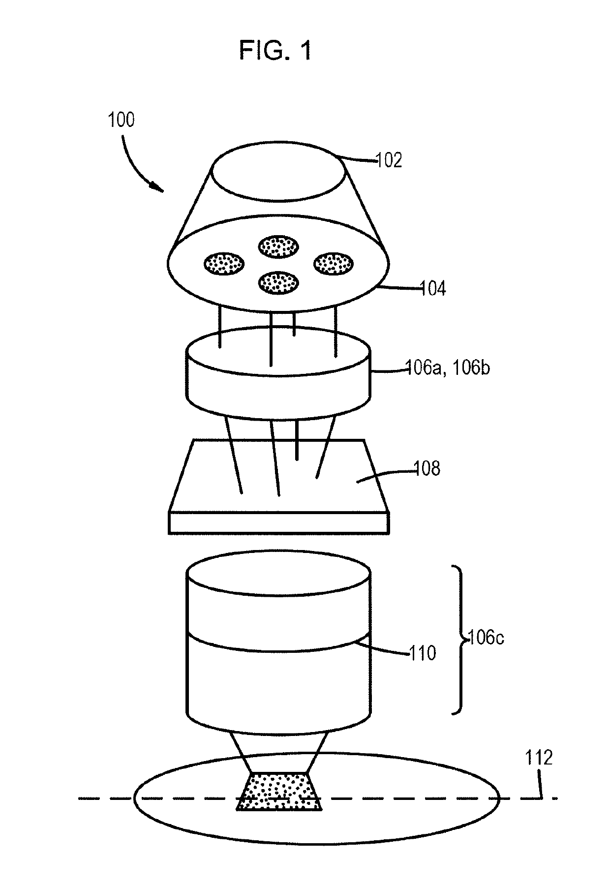
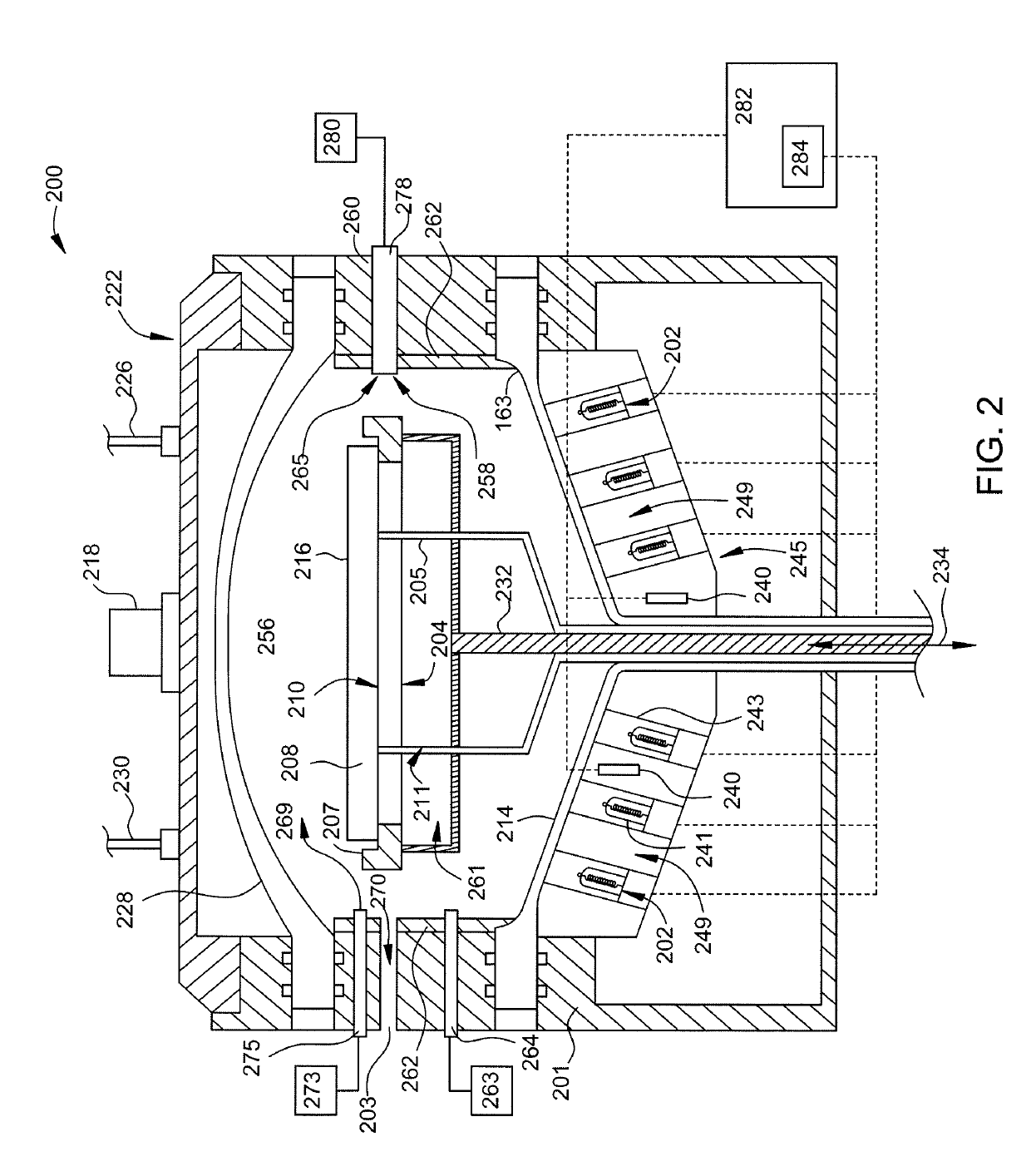
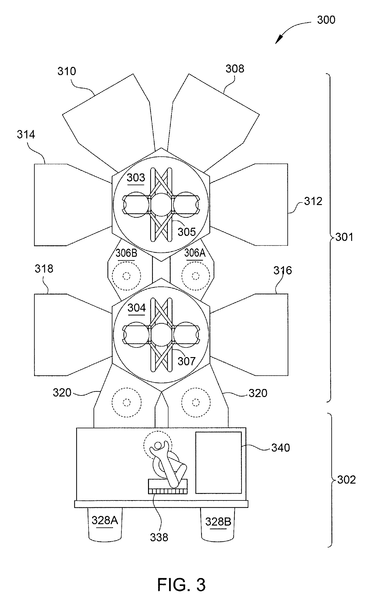
[0020]The following disclosure describes methods for detecting excursions in intended geometric features in an integrated circuit substrate. Certain details are set forth in the following description and in FIGS. 1-7 to provide a thorough understanding of various implementations of the disclosure. Other details describing well-known structures and systems often associated with plasma etching are not set forth in the following disclosure to avoid unnecessarily obscuring the description of the various implementations.

[0021]Many of the details, dimensions, components, and other features shown in the Figures are merely illustrative of particular implementations. Accordingly, other implementations can have other details, components, dimensions, angles and features without departing from the spirit or scope of the present disclosure. In addition, further implementations of the disclosure can be practiced without several of the details described below.

[0022]In semiconductor fabrication, ea...


PUM


Abstract

Implementations described herein generally relate to detecting excursions in intended geometric features in an integrated circuit substrate. In one implementation, a method includes determining a set of suspect contours in a design window of the integrated circuit substrate based on proximities of a plurality of points of interest in the design window to intended geometric features. The method further includes obtaining a set of imaged contours from one or more images of a defect-free integrated circuit substrate. The method further includes comparing the set of imaged contours to the set of suspect contours to obtain a set of potential excursions from the imaged contours. The method further includes determining a probability that a potential excursion from the set of potential excursions is a valid excursion. The method further includes taking a corrective action based on the determined probability.

Description

BACKGROUNDField[0001]Implementations described herein generally relate to automatically detecting excursions in intended geometric features in an integrated circuit substrate.Description of the Related Art[0002]Manufacturing silicon substrates involves a series of steps, which may include lithography, etching, deposition, and planarization, each of which may be repeated for a plurality of layers. Lithographic apparatuses may employ a mask that may contain a circuit pattern corresponding to an individual layer of an integrated circuit, and this pattern can be imaged onto a target portion (e.g. comprising one or more dies) on a substrate (silicon substrate) that has been coated with a layer of radiation-sensitive material (resist). In general, a single substrate will contain a whole network of adjacent target portions that are successively irradiated via the projection system, one at a time. In one type of lithographic projection apparatus, each target portion is irradiated by exposin...

Claims


Application Information

Patent Timeline
Patent Type & Authority Applications(United States)
IPC IPC(8): G01R31/28G06T7/60G06F17/50G06F17/30G01R31/3185
CPCG01R31/2862G06T7/60G06F16/5838G06F17/5072G01R31/318516G06T7/001G06T2207/10056G06T2207/30148G06F30/392G06F2119/18Y02P90/02
Inventor NURANI, RAMAN K.SETHURAMAN, ANANTHA R.RAGAVAN, KOUSHIK
Owner APPLIED MATERIALS INC
Why Eureka
Try Eureka