

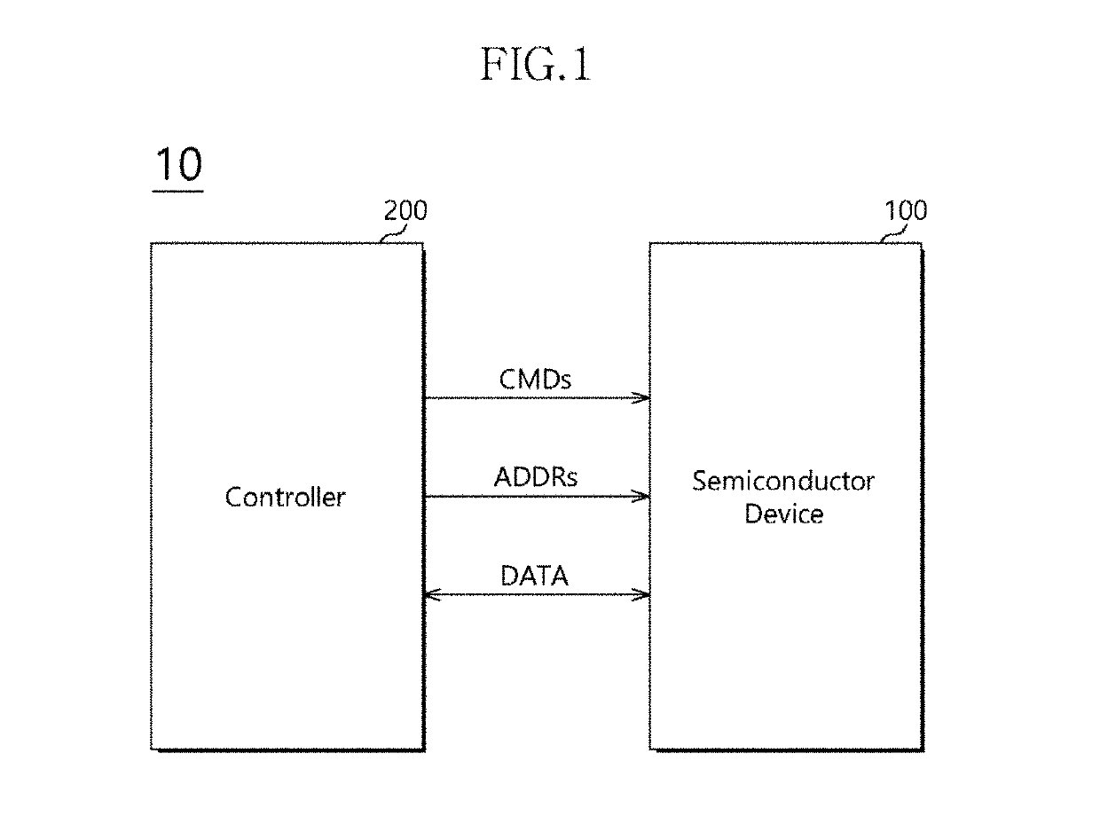
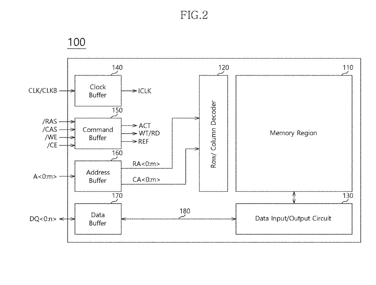
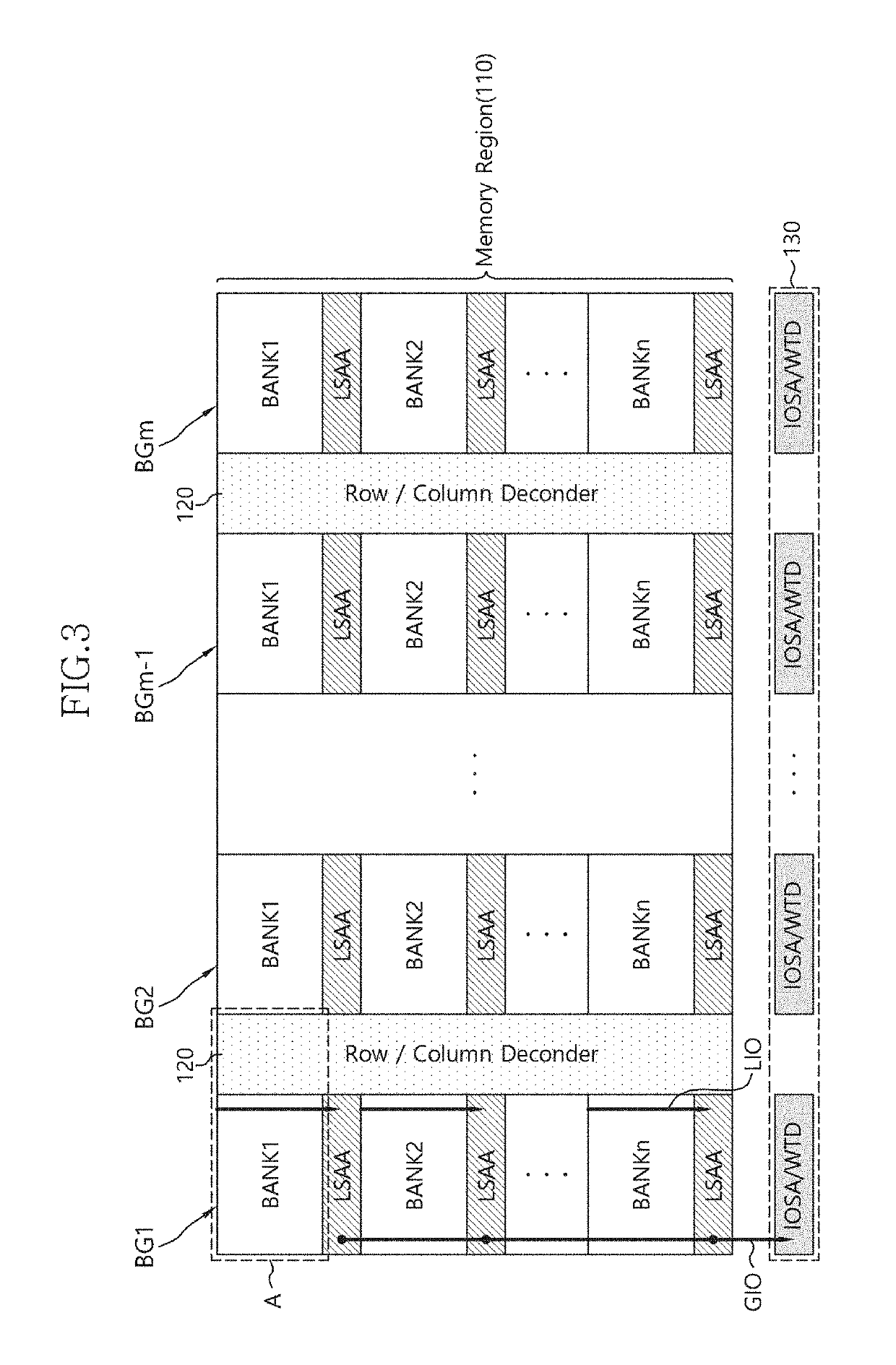
Semiconductor device
a memory device and semiconductor technology, applied in the field can solve the problems of affecting the high integration of semiconductor memory devices, and achieve the effects of improving the quantity of data simultaneously input/output from/from a single mat, low power consumption, and small siz
- Summary
- Abstract
- Description
- Claims
- Application Information
AI Technical Summary
Benefits of technology
Problems solved by technology
Method used
Image

Examples
Embodiment Construction
[0030]Various embodiments of the present invention are described below in more detail with reference to the accompanying drawings. We note, however, that the present invention may be embodied in different forms and variations, and should not be construed as being limited to the embodiments set forth herein. Rather, the described embodiments are provided so that this disclosure will be thorough and complete, and will fully convey the present invention to those skilled in the art to which this invention pertains. Throughout the disclosure, like reference numerals refer to like parts throughout the various figures and embodiments of the present invention. It is noted that reference to “an embodiment” does not necessarily mean only one embodiment, and different references to “an embodiment” are not necessarily to the same embodiment(s).
[0031]The drawings are not necessarily to scale and, in some instances, proportions may have been exaggerated in order to clearly illustrate features of ...
PUM
 Abstract
Description
Claims
Application Information