Electronic package and method for fabricating the same

a technology of electronic packaging and packaging method, which is applied in the direction of semiconductor/solid-state device details, semiconductor devices, electrical apparatus, etc., can solve the problems of limited function and efficiency of semiconductor packages b>1/b>, and achieve the effect of high efficiency

Active Publication Date: 2019-08-01
SILICONWARE PRECISION IND CO LTD
View PDF5 Cites 7 Cited by
  • Summary
  • Abstract
  • Description
  • Claims
  • Application Information

AI Technical Summary

Benefits of technology

[0021]According to the present disclosure, since the first electronic component and the second electronic component are arranged on upper and lower sides of the second circuit structure, respectively, the electronic package can provide multi-function and high efficiency.

Problems solved by technology

However, since the semiconductor elements 11 are disposed on a single side of the circuit structure 16, the function and efficiency of the semiconductor packages 1 are limited.
Therefore, the function and efficiency of the end electronic products are limited.

Method used


Image

  • Electronic package and method for fabricating the same
  • Electronic package and method for fabricating the same
  • Electronic package and method for fabricating the same

Examples


Embodiment Construction

[0026]The following illustrative embodiments are provided to illustrate the disclosure of the present disclosure, these and other advantages and effects can be apparent to those in the art after reading this specification.

[0027]It should be noted that all the drawings are not intended to limit the present disclosure. Various modifications and variations can be made without departing from the spirit of the present disclosure. Further, terms such as “first”, “second”, “on”, “a” etc. are merely for illustrative purposes and should not be construed to limit the scope of the present disclosure.

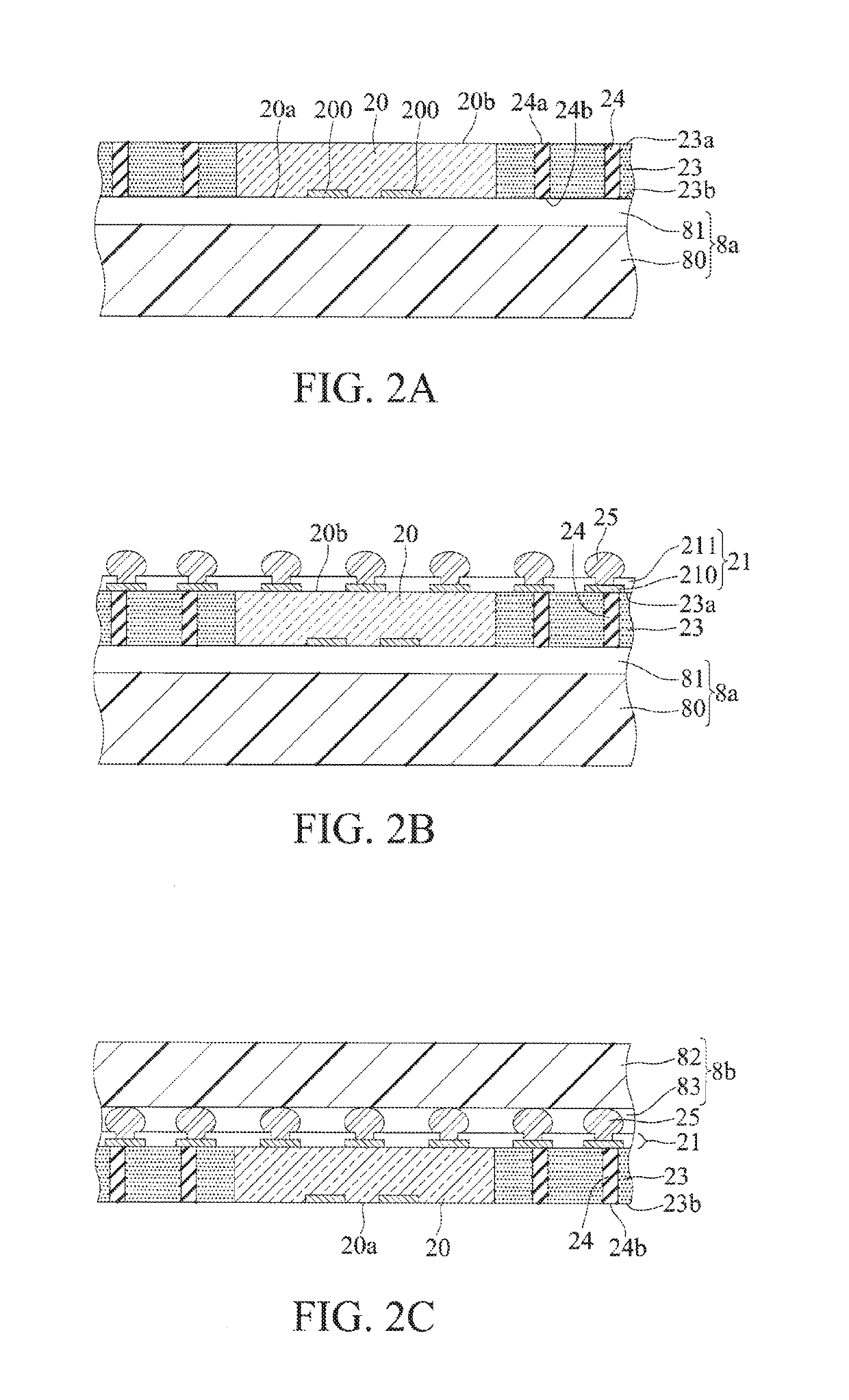
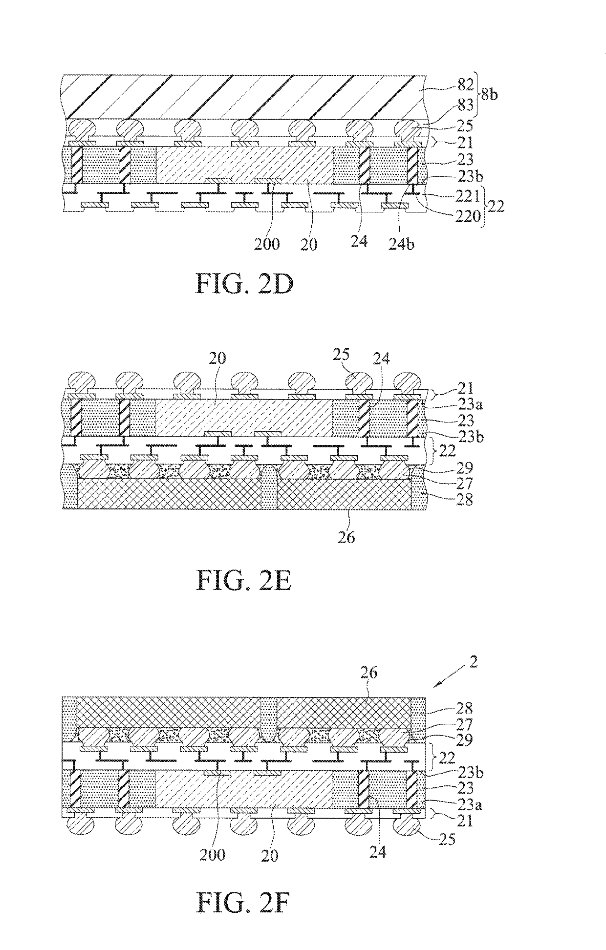
[0028]FIGS. 2A to 2F are schematic cross-sectional views showing a method for fabricating an electronic package 2 according to a first embodiment of the present disclosure.

[0029]Referring to FIG. 2A, a first carrier 8a is provided, a plurality of conductive posts 24 are disposed on the first carrier 8a, and at least a first electronic component 20 is disposed on the first carrier 8a. Then, a first ...


PUM


Abstract

An electronic package and a method for fabricating the same are provided. The method includes: forming a circuit structure on an encapsulant; embedding a first electronic component and a plurality of conductive posts in the encapsulant; and disposing a second electronic component on the circuit structure. Since the first and second electronic components are arranged on opposite sides of the circuit structure, the electronic package can provide multi-function and high efficiency.

Description

BACKGROUND1. Technical Field[0001]The present disclosure relates to packaging processes, and, more particularly, to an electronic package having a plurality of chips and a method for fabricating the electronic package.2. Description of Related Art[0002]Along with the rapid development of electronic industries, electronic products are developed toward the trend of multi-function and high performance. Accordingly, wafer level packaging (WLP) technologies have been developed to meet the miniaturization requirement of electronic packages.[0003]FIGS. 1A to 1E are schematic cross-sectional views showing a method for fabricating a semiconductor package 1 using WLP technologies according to the prior art.[0004]Referring to FIG. 1A, a thermal release tape 100 is formed on a carrier 10.[0005]Then, a plurality of semiconductor elements 11 are disposed on the thermal release tape 100. Each of the semiconductor elements 11 has an active surface 11a with a plurality of electrode pads 110 disposed...

Claims


Application Information

Patent Timeline
Patent Type & Authority Applications(United States)
IPC IPC(8): H01L23/31H01L23/522H01L23/00H01L25/065
CPCH01L23/3114H01L23/5226H01L23/3128H01L24/06H01L24/14H01L25/0657H01L23/49838H01L23/49816H01L21/4853H01L25/16H01L24/19H01L24/20H01L2224/73204H01L2224/16225H01L2924/18161H01L2224/32225H01L2224/73267H01L2224/13101H01L2224/13147H01L24/13H01L2224/1134H01L2924/181H01L2224/81385H01L2224/18H01L21/6835H01L2221/68359H01L2221/68372H01L21/568H01L2924/00014H01L24/73H01L24/32H01L24/16H01L2924/15311H01L2924/014H01L2924/00012H01L2224/29099H01L2924/00H01L23/481H01L23/5383H01L23/5389H01L25/0652H01L21/563H01L21/561H01L21/56H01L21/31051
Inventor HUANG, CHEN-YUCHUNG, CHEE-KEYLIN, CHANG-FUNG, KONG-TOONTAI, RUI-FENGMA, BO-HAO
Owner SILICONWARE PRECISION IND CO LTD
Why Eureka
Try Eureka