Dram cell array using facing bar and method of fabricating the same

a dram cell and facing bar technology, applied in the direction of electrical equipment, semiconductor devices, capacitors, etc., can solve the problem of limiting the layout area of the dram cell, and achieve the effect of reducing the overall layout area

US20190237467A1Active Publication Date: 2019-08-01DOSILICON CO LTD
2 Cites 5 Cited by

Patent Information

Authority / Receiving Office
US · United States
Current Assignee / Owner
Publication Date
2019-08-01

Smart Images

  • Figure 1
    Figure 1
  • Figure 2
    Figure 2
  • Figure 3
    Figure 3
Patent Text Reader

Abstract

A dynamic random access memory (DRAM) cell array using facing bars and a method of fabricating the DRAM cell array are disclosed. A first DRAM cell and a second DRAM cell of each of DRAM cell pairs of a DRAM cell array fabricated using a method of fabricating a DRAM cell array share a facing bar and a bit line plug therebetween. Thus, the overall layout area is greatly reduced by a DRAM cell array fabricated using the method of fabricating the DRAM cell array. Further, in the method of fabricating the DRAM cell array, a storage of each of the DRAM cells of the DRAM cell array is formed as a multi-fin type having a plurality of lateral protrusions, thereby greatly increasing an area of the storage.
Need to check novelty before this filing date? Find Prior Art

Description

CROSS-REFERENCE TO RELATED APPLICATION

[0001] This application claims priority to and the benefit of Korean Patent Application No. 10-2018-0010391, filed on Jan. 29, 2018, the disclosure of which is incorporated herein by reference in its entirety.BACKGROUND1. Field of the Invention

[0002] The present invention relates to a dynamic random access memory (DRAM) cell array and a method of fabricating the same, and more particularly, to a DRAM cell array using facing bars and a method of fabricating the DRAM cell array.2. Discussion of Related Art

[0003] Generally, a dynamic random access memory (DRAM) is formed to include a plurality of DRAM cells. At this point, each of the plurality of DRAM cells is configured with a single cell transistor and a single storage. The storage is able to store charges, and the cell transistor forms a transmission channel for conducting between a bit line and the storage according to a voltage applied to a gate electrode.

[0004] Meanwhile, as DRAMs become highly ...

Examples

Embodiment Construction

[0018]Exemplary embodiments of the present invention will be described in detail below with reference to the accompanying drawings. While the present invention is shown and described in connection with the exemplary embodiments thereof, it will be apparent to those skilled in the art that various modifications can be made without departing from the spirit and scope of the invention.

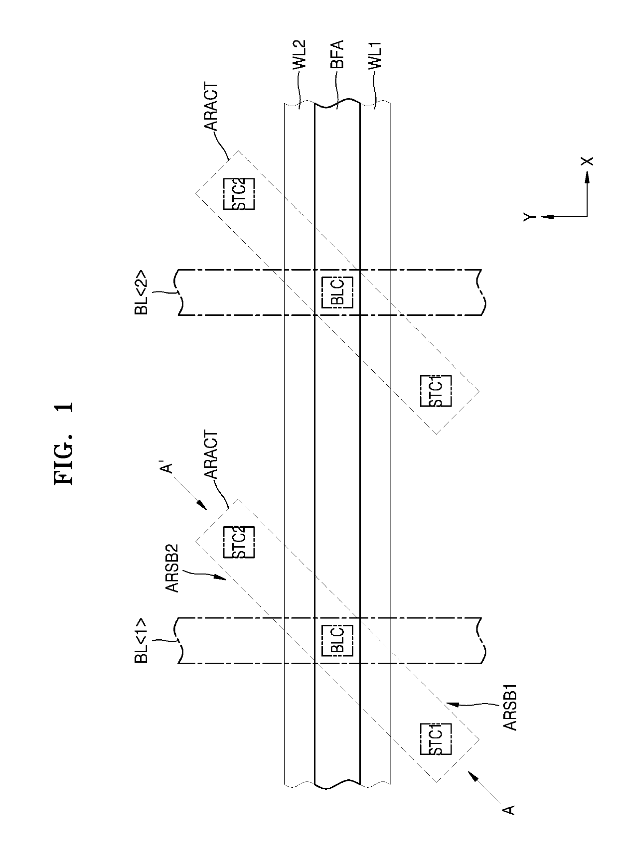
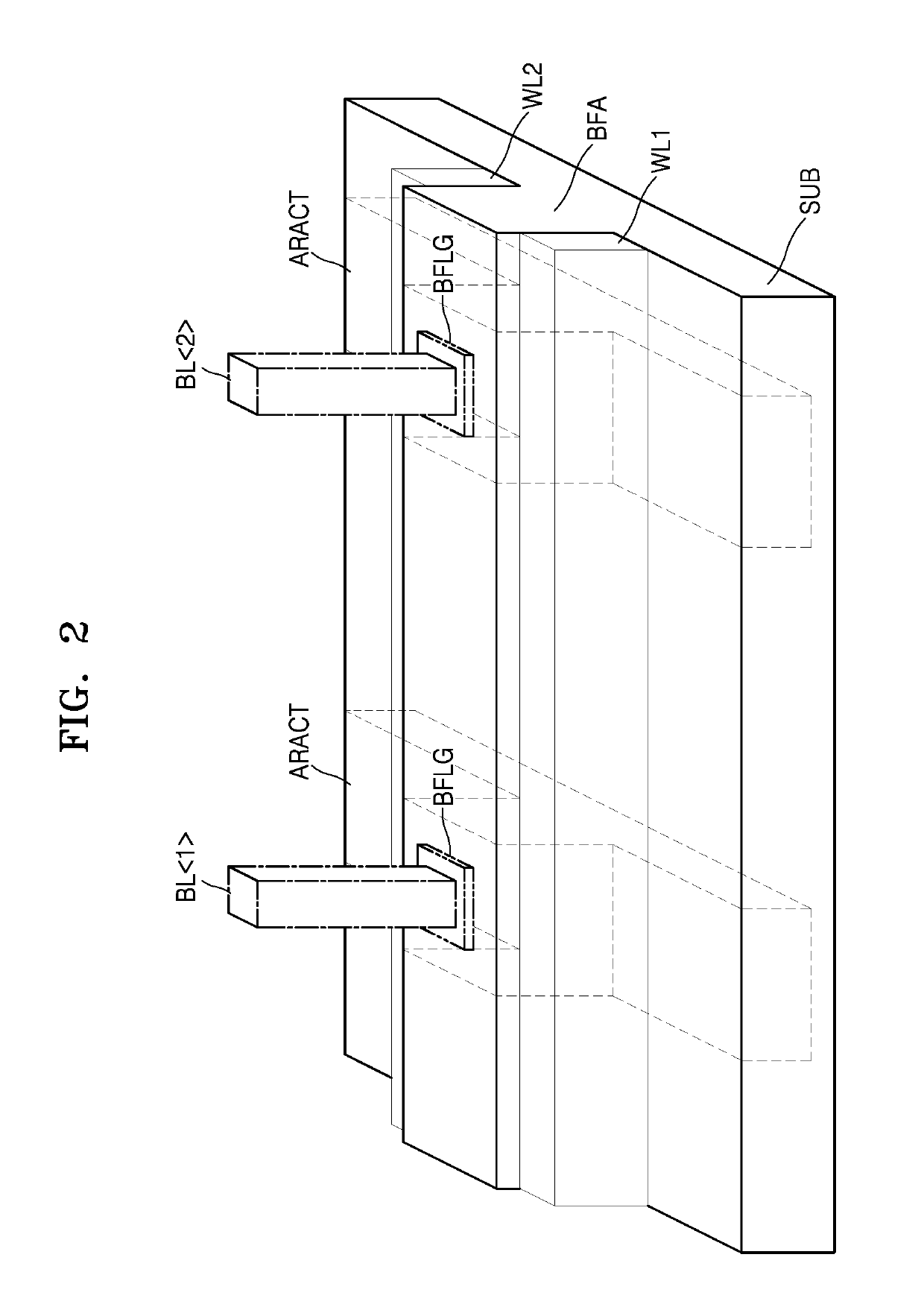
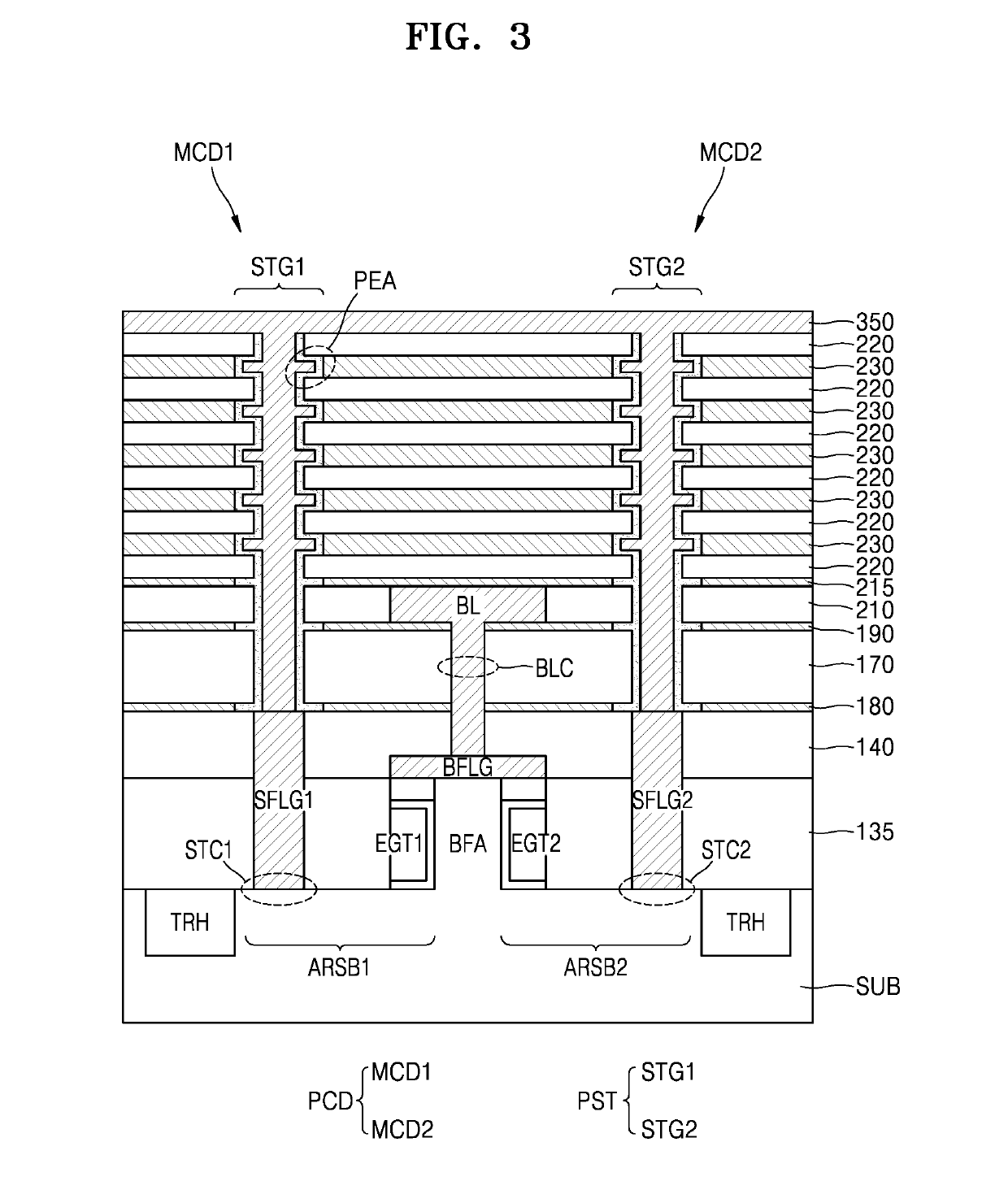
[0019]FIG. 1 is a layout diagram of a portion of a dynamic random access memory (DRAM) cell array according to an exemplary embodiment of the present invention. FIG. 2 is a perspective view of the DRAM cell array of FIG. 1, and for the sake of clarity, only some components are illustrated. FIG. 3 is a cross-sectional view taken along a line A-A′ of FIG. 1.

[0020]Referring to FIGS. 1 to 3, a plurality of DRAM cell pairs may be arranged in a DRAM cell array according to the present invention. Each of the plurality of DRAM cell pairs PCD may include a first DRAM cell MCD1 and a second DRAM cell MCD2.

[0021]Fur...