Layout structure of semiconductor device

a semiconductor device and layout structure technology, applied in semiconductor devices, semiconductor/solid-state device details, instruments, etc., can solve the problems of reducing the number of reinforcing power supply cells to be arranged, the leakage current in the off-state transistor has been increased to a nonnegligible level, and the process size is important, so as to reduce the number of reinforcing power supply cells to be arranged, the layout area is increased, and the chip area is reduced

Inactive Publication Date: 2008-07-17
SOCIONEXT INC
View PDF8 Cites 43 Cited by
  • Summary
  • Abstract
  • Description
  • Claims
  • Application Information

AI Technical Summary

Benefits of technology

[0033]According to the sixth aspect of the present invention, in the structure in which the power supply wire and the substrate or well potential wire are shared between adjacent ones of the cell lines, the reinforcing power supply cell is arranged in every second cell line of the plurality of the cell lines. Thus, an object of independent supply of a stable potential as a substrate or well potential from a power supply potential can be achieved and also the number of reinforci

Problems solved by technology

In recent years, reduction in stand-by current in an LSI using MOS (metal oxide semiconductor) transistors has been an important issue.
However, due to reduction in process size and reduction in threshold voltage resulting from the development of low voltage LSIs, leakage currents in transistors in OFF state have been increased to a nonnegligible level.
Accordingly, a substrate or well potential is not stable and a threshold in a transistor fluctuates, or like inconvenience occurs.
This causes problems such as reduction in reliability of an LSI operation, insufficient suppression of a stand-by leakage current and the like.
However, the known layout structure has the following problems.
However, it has become clear that as the process size has been reduced, a maximum effect of reduction of a leakage current by controlling a substrate or well potential can

Method used


Image

  • Layout structure of semiconductor device
  • Layout structure of semiconductor device
  • Layout structure of semiconductor device

Examples


first embodiment

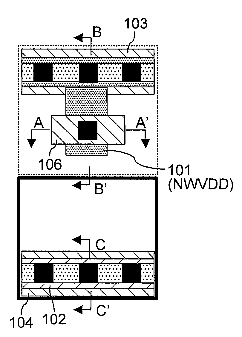
[0056]FIGS. 1A through 1D are views illustrating a layout structure of a reinforcing power supply cell according to this embodiment. FIG. 1A is a plan view of the layout structure. FIG. 1B is a cross-sectional view taken along the line A-A′ of FIG. 1A. FIG. 1C is a cross-sectional view taken along the line B-B′ of FIG. 1A. FIG. 1D is a cross-sectional view taken along the line C-C′ of FIG. 1A.

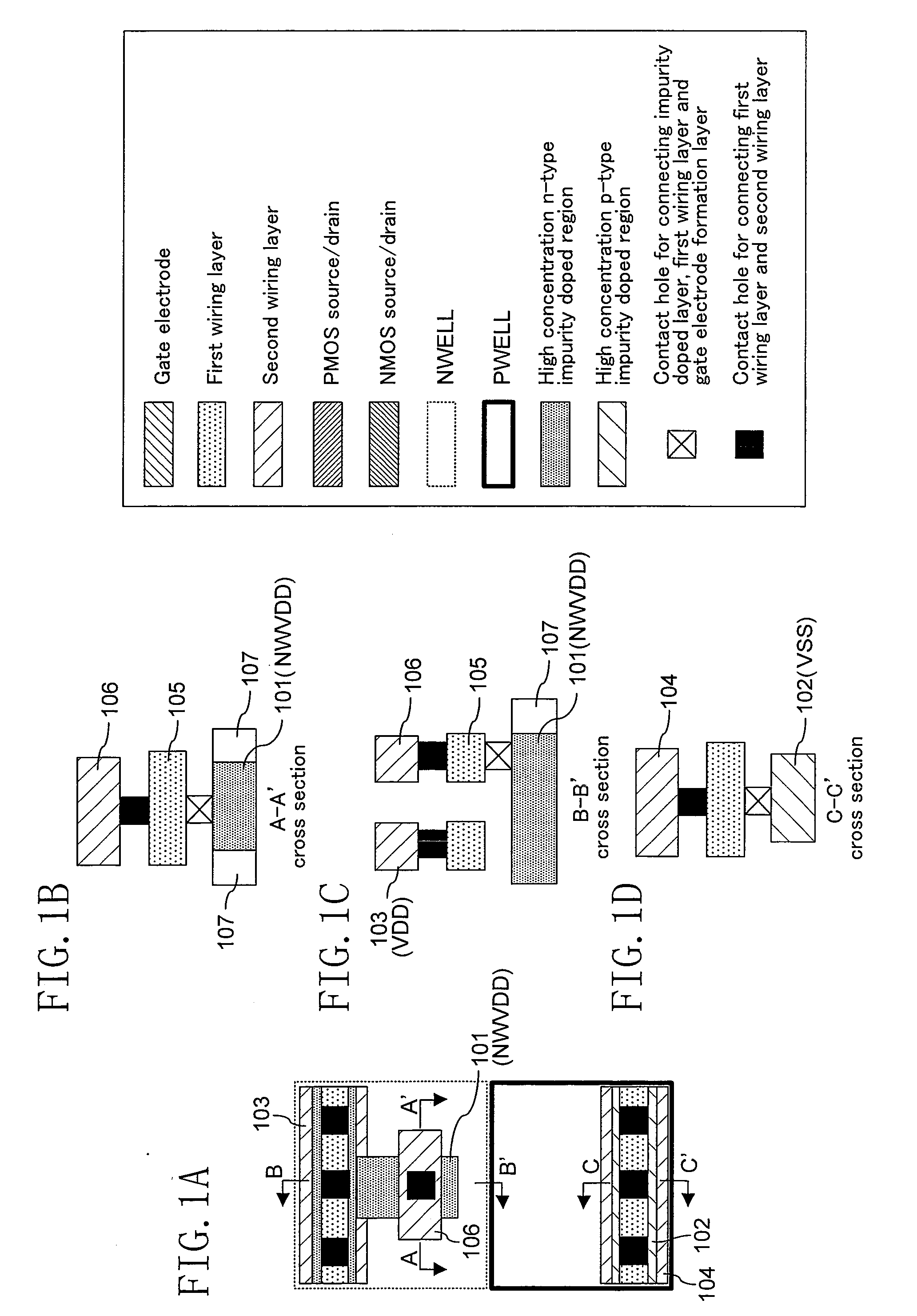
[0057]FIGS. 2A through 2E are views illustrating a layout structure of a cell constituting a semiconductor device according to this embodiment. FIG. 2A is a plan view of the layout structure. FIG. 2B is a cross-sectional view taken along the line D-D′ of FIG. 2A. FIG. 2C is a cross-sectional view taken along the line E-E′ of FIG. 2A. FIG. 2D is a cross-sectional view taken along the line F-F′ of FIG. 2A. FIG. 2E is a cross-sectional view taken along the line G-G′ of FIG. 2A.

[0058]The cell of FIGS. 2A through 12E is formed so as to have a structure in which in an n-well side, i.e., a p-type tran...

second embodiment

[0070]FIGS. 4A through 4D are views illustrating a layout structure of a reinforcing power supply cell according to this embodiment. FIG. 4A is a plan view of the layout structure. FIG. 4B is a cross-sectional view taken along the line H-H′ of FIG. 4A. FIG. 4C is a cross-sectional view taken along the line I-I′ of FIG. 4A. FIG. 4D is a cross-sectional view taken along the line J-J′ of FIG. 4A.

[0071]As described in the first embodiment, by combining the reinforcing power supply cell of FIGS. 1A through 1D and the cell of FIGS. 2A through 2E as shown in FIG. 3, a semiconductor device which allows only in a p-transistor arranging region independent supply of the substrate or well potential NWVDD from the positive power supply potential VDD and reinforcement of the substrate or well potential NWVDD can be achieved.

[0072]In contrast, by using the reinforcing power supply cell of FIGS. 4A through 4D, a semiconductor device which allows only in an n-type transistor arranging region indepen...

third embodiment

[0076]FIGS. 5A through 5E are views illustrating a layout structure of a reinforcing power supply cell according to this embodiment. FIG. 5A is a plan view of the layout structure. FIG. 5B is a cross-sectional view taken along the line K-K′ of FIG. 5A. FIG. 5C is a cross-sectional view taken along the line L-L′ of FIG. 5A. FIG. 5D is a cross-sectional view taken along the line M-M′ of FIG. 5A. FIG. 5E is a plan view illustrating a layout structure of a reinforcing power supply cell according to a modified example of the third embodiment.

[0077]The reinforcing power supply cell of FIGS. 5A through 5D corresponds to a cell having a layout structure of FIGS. 12A through 12E, i.e., a layout structure obtained by combination of the reinforcing power supply cell of FIGS. 1A through 1D and the reinforcing power supply cell of FIGS. 4A through 4D.

[0078]Specifically, a first power supply impurity doped region 505 is electrically connected to the high concentration n-type impurity doped region...


PUM


Abstract

In a layout structure capable of independent supply of a substrate or well potential from a power supply potential, further reduction in layout area is achieved. A reinforcing power supply cell is inserted in a cell line in which a plurality of cells are arranged in series. Each of the cells includes an impurity doped region for supplying a substrate or well potential NWVDD which is different from a positive power supply potential VDD to a p-type transistor arranging region. The reinforcing power supply cell includes a power supply impurity doped region to which an impurity doped region of an adjacent cell is electrically connected and a power supply wire provided in a wiring layer formed above the power supply impurity doped region and electrically connected to the power supply impurity doped region.

Description

CROSS-REFERENCE TO RELATED APPLICATION[0001]The disclosure of Japanese Patent Application No. 2007-4662 filed on Jan. 12, 2007, including specification, drawings and claims is incorporated herein by reference in its entirety.BACKGROUND OF THE INVENTION[0002]1. Field of the Invention[0003]The present invention relates to a layout structure for a semiconductor device, and more particularly relates to a layout structure capable of independent supply of a substrate or well potential from a power supply potential.[0004]2. Description of the Related Art[0005]In recent years, reduction in stand-by current in an LSI using MOS (metal oxide semiconductor) transistors has been an important issue. However, due to reduction in process size and reduction in threshold voltage resulting from the development of low voltage LSIs, leakage currents in transistors in OFF state have been increased to a nonnegligible level.[0006]To cope with such problems, there has been a known method in which a leakage ...

Claims


Application Information

Patent Timeline
IPC IPC(8): G05F3/02
CPCH01L27/092H01L27/0207
Inventor TOUBOU, TETSUROU
Owner SOCIONEXT INC
Why Eureka
Try Eureka