Liquid crystal panel and method for manufacturing the same

Inactive Publication Date: 2019-08-08
TCL CHINA STAR OPTOELECTRONICS TECH CO LTD
View PDF5 Cites 0 Cited by
  • Summary
  • Abstract
  • Description
  • Claims
  • Application Information

AI Technical Summary

Benefits of technology

[0005]The liquid crystal panel according to the present disclosure can effectively prevent an overlap between a PI and a sealant, namely effectively preventing the sealant peeling and improving the qualified rate of products.
[0012]In the liquid crystal panel according to the present disclosure, the color-resistance layer is provided thereon with a second passivation layer that can protect the color-resistance layer.
[0020]In the liquid crystal panel of the present disclosure, the retaining wall provided on the color filter substrate of can effectively prevent an overlap between the PI and the sealant, thereby preventing sealant peeling and improving the qualified rate of products. The method for manufacturing the liquid crystal panel of the present disclosure can effectively produce the retaining wall. Operation is easy and it does not have any adverse impact on the quality of the black matrix layer and the ITO layer of the color filter substrate.

Problems solved by technology

In a panel designed with a narrow bezel, due to a short distance between the edge of the active area and the sealant as well as a deviation of the PI coating, the PI and the sealant can easily overlap, thus resulting in sealant peeling, causing serious product problems such as no-display and low qualified rate of products.

Method used


Image

  • Liquid crystal panel and method for manufacturing the same
  • Liquid crystal panel and method for manufacturing the same
  • Liquid crystal panel and method for manufacturing the same

Examples


Embodiment Construction

[0027]Details of the present disclosure will be more apparent from the following description of the accompanying drawings and the embodiments of the present disclosure. However, the embodiments of the present disclosure described herein are for the purpose of explaining the present disclosure and are not to be construed as limiting the present disclosure in any manner. It will be apparent to those skilled in the art that those skilled in the art may contemplate any possible variations based on the present disclosure, which are to be considered as falling within the scope of the present disclosure, which will be further described below with reference to the accompanying drawings.

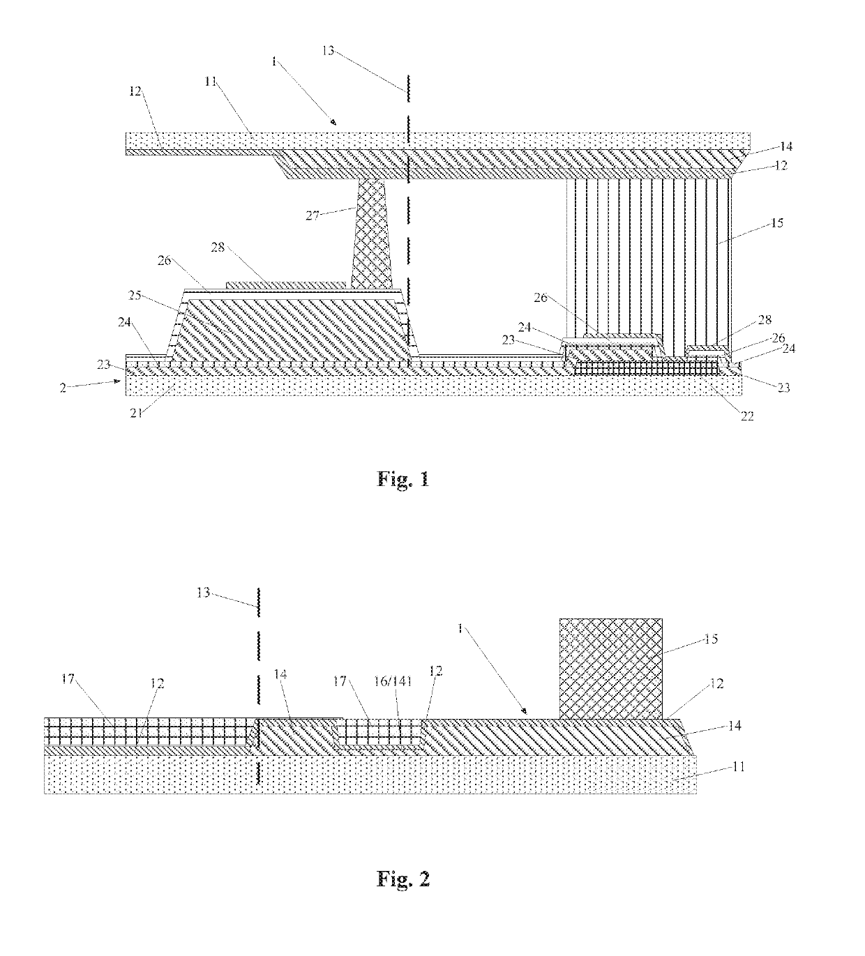
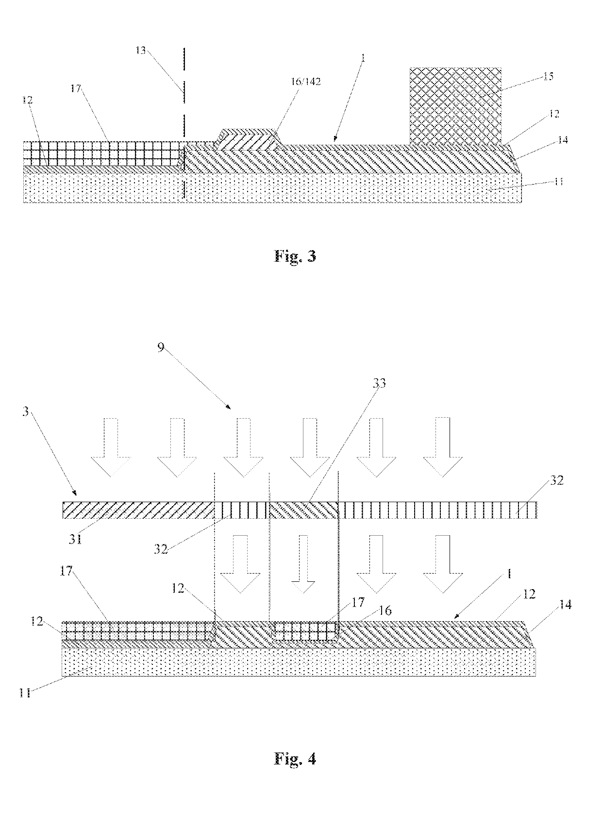
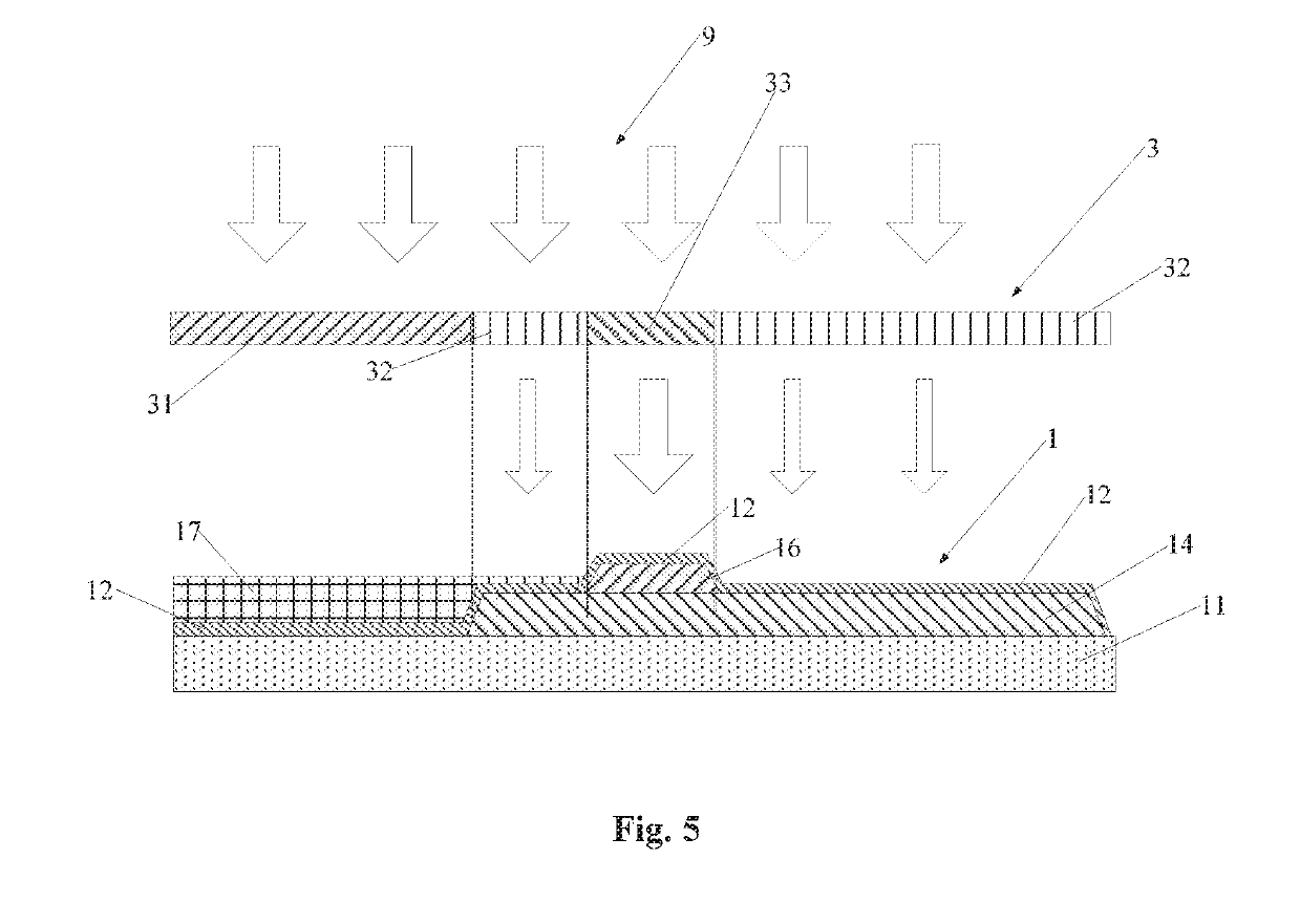
[0028]FIGS. 1 to 5 are respectively a schematic view of the structure of a liquid crystal panel, a schematic view of a structure of a color filter substrate of the present disclosure, a schematic view of another structure of the color filter substrate of the present disclosure, a schematic view of a manufactu...


PUM


Abstract

Disclosed is a liquid crystal panel. The liquid crystal panel comprises a color filter substrate. The color filter substrate comprises a first glass layer, on which a protective layer is provided. An edge of an active area of the color filter substrate is provided thereon with a black matrix layer and a sealant layer. The black matrix layer is located between the first glass layer and the protective layer. A length of the black matrix layer is smaller than that of the first glass layer. A retaining wall is provided on an upper surface of the black matrix layer, and a sealant layer is arranged at an end of the protective layer. The liquid crystal panel can effectively prevent an overlap between a PI liquid and the sealant, thereby preventing sealant peeling and improving the qualified rate of products.

Description

CROSS-REFERENCE TO RELATED APPLICATIONS[0001]The present application claims the priority of Chinese patent application CN201610934887.0, entitled “Liquid Crystal Panel and Method for Manufacturing the Same”, and filed on Nov. 1, 2016, the entirety of which is incorporated herein by reference.FIELD OF THE DISCLOSURE[0002]The present disclosure relates to the technical field of liquid crystal display, and in particular to a liquid crystal panel and a method for manufacturing the same.BACKGROUND OF THE DISCLOSURE[0003]In manufacturing a liquid crystal panel, the active area is normally coated with a PI liquid to achieve liquid-crystal alignment. At present, the mainstream liquid crystal panels are designed with narrow bezels and curved surfaces, and the corresponding designs are usually POA (PS on Array) or COA (Color Filter on Array). In a panel designed with a narrow bezel, due to a short distance between the edge of the active area and the sealant as well as a deviation of the PI co...

Claims


Application Information

Patent Timeline
IPC IPC(8): G02F1/1335G02F1/1339
CPCG02F1/133514G02F1/133512G02F1/1339G02F2201/50G02F1/13394G02F1/133388
Inventor YING, JIANJIANDU, PENG
Owner TCL CHINA STAR OPTOELECTRONICS TECH CO LTD
Why Eureka
Try Eureka