

Conductive beam optic containing internal heating element
a beam optic and heating element technology, applied in the field of conductive beam optics, can solve the problems of increased likelihood of particulate contamination on the wafer, spiking in the dc potential during operation, and time-consuming maintenance processes, and achieve the effect of reducing particle build-up
- Summary
- Abstract
- Description
- Claims
- Application Information
AI Technical Summary
Benefits of technology
Problems solved by technology
Method used
Image

Examples
Embodiment Construction
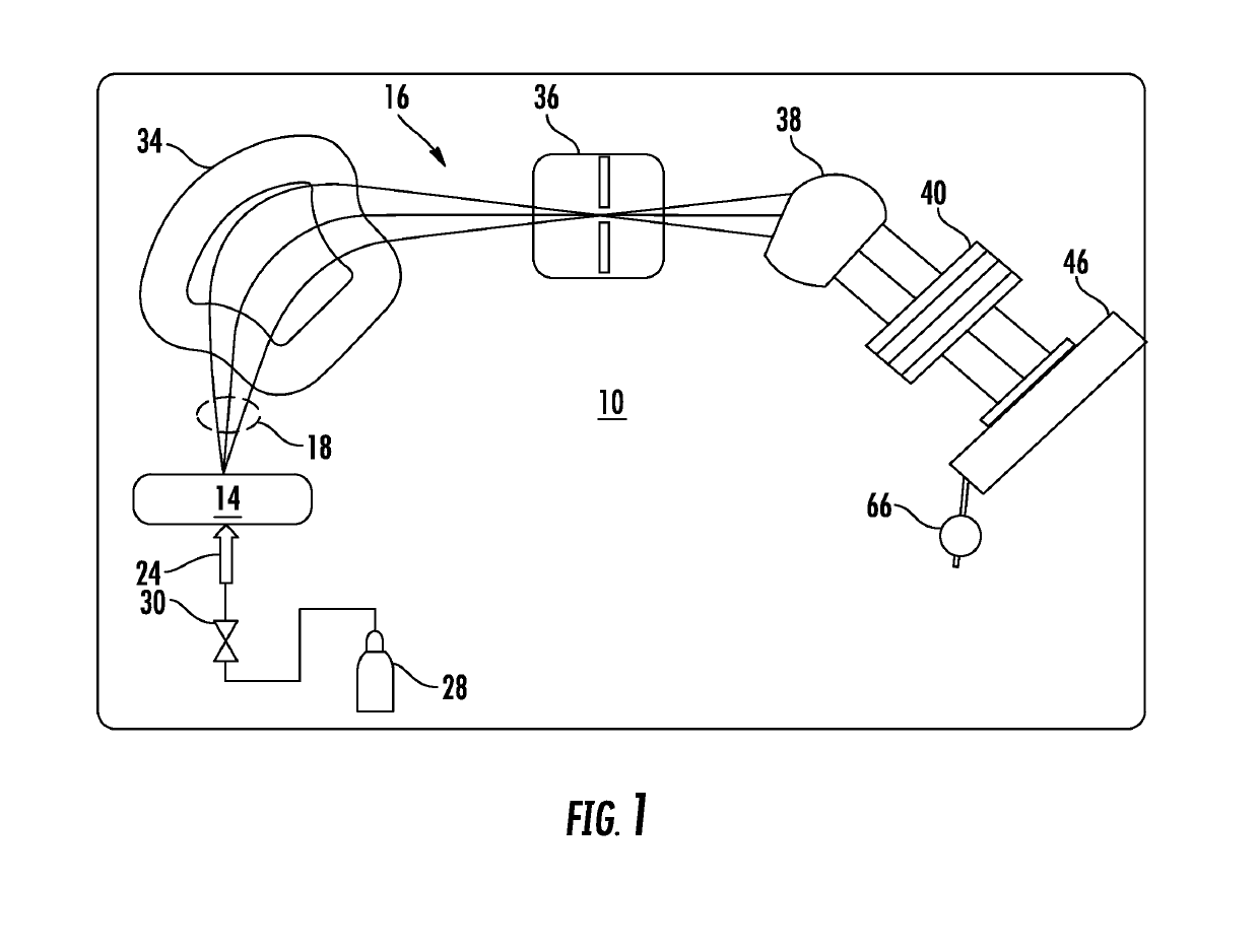
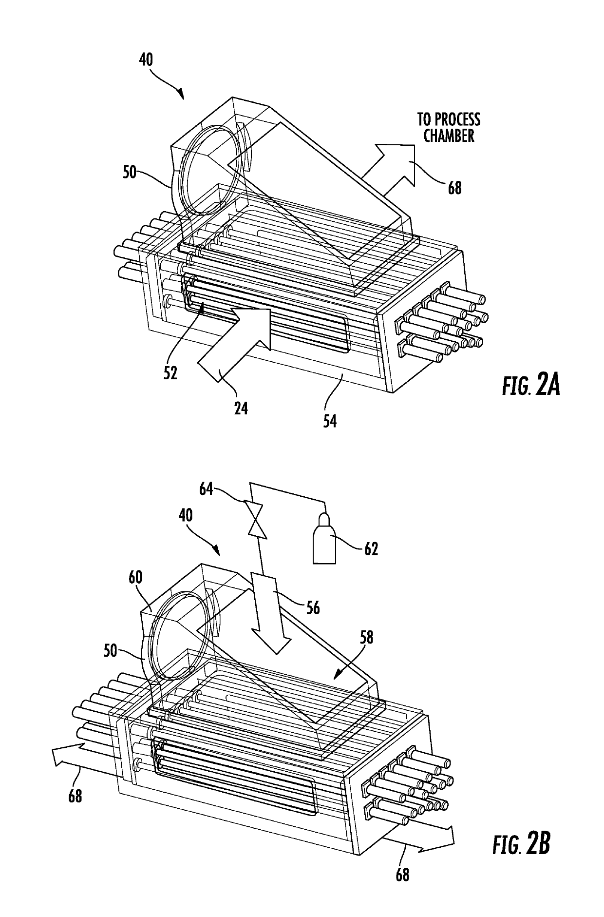
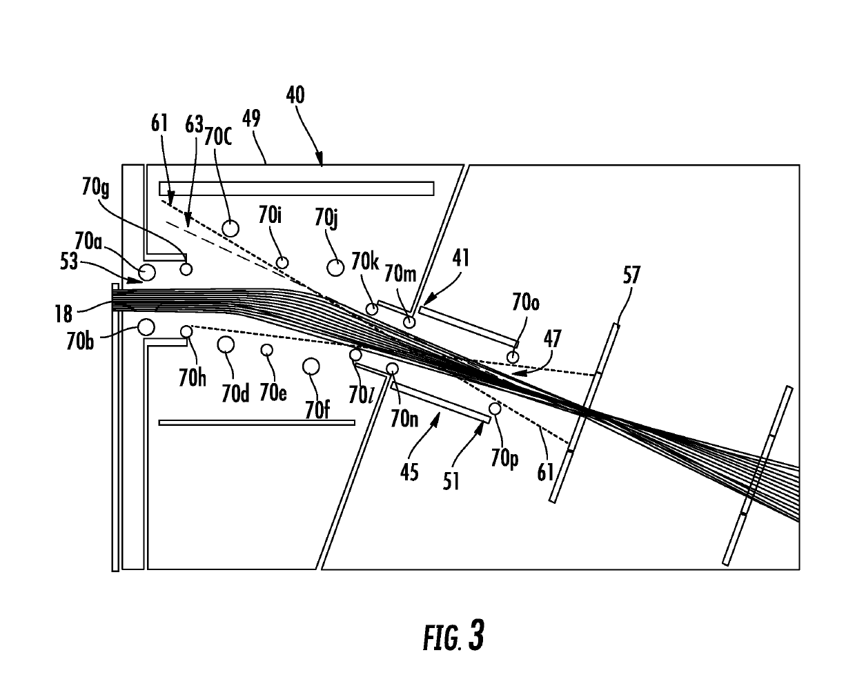
[0019]A system and method in accordance with the present disclosure will now be described more fully hereinafter with reference to the accompanying drawings, where embodiments of the system and method are shown. The system and method may be embodied in many different forms and are not be construed as being limited to the embodiments set forth herein. Instead, these embodiments are provided so the disclosure will be thorough and complete, and will fully convey the scope of the system and method to those skilled in the art.
[0020]For the sake of convenience and clarity, terms such as “top,”“bottom,”“upper,”“lower,”“vertical,”“horizontal,”“lateral,” and “longitudinal” will be used herein to describe the relative placement and orientation of various components and their constituent parts, as appearing in the figures. The terminology will include the words specifically mentioned, derivatives thereof, and words of similar import.
[0021]As used herein, an element or operation recited in the ...
PUM
 Abstract
Description
Claims
Application Information