Organic light emitting diode display device and manufacturing method thereof

Active Publication Date: 2019-10-10
TCL CHINA STAR OPTOELECTRONICS TECH CO LTD
View PDF1 Cites 3 Cited by
  • Summary
  • Abstract
  • Description
  • Claims
  • Application Information

AI Technical Summary

Benefits of technology

The present invention provides an organic light emitting diode display device and a manufacturing method that can reduce the risk of breakage of the barrier layer and the buffer layer, and improve the service life of the OLED display device. The invention achieves this by disposing a water absorbing material layer in the barrier layer, which prevents water and oxygen from penetrating into the device and reduces water-oxygen permeability. This helps prevent damage to the device and improves its durability.

Problems solved by technology

However, since the thin film barrier layer and the buffer layer are thin, there is a stress between the layers.
Therefore, the ability of the barrier layer and the buffer layer for blocking water and oxygen does not achieve the desired effect.
The water-oxygen permeability is high, and the barrier layer and the buffer layer are more likely to break and cause the package to fail.

Method used


Image

  • Organic light emitting diode display device and manufacturing method thereof
  • Organic light emitting diode display device and manufacturing method thereof

Examples


Embodiment Construction

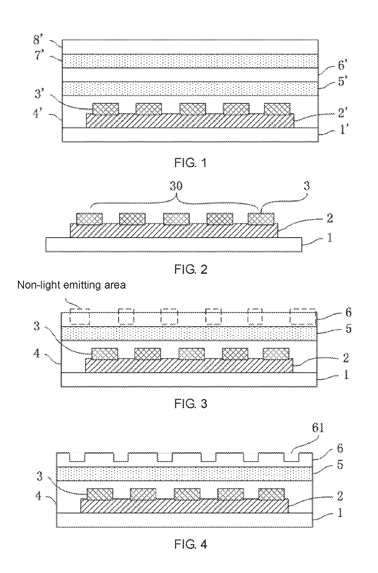
[0054]The present invention provides a manufacturing method of an organic light emitting diode (OLED) display device, comprising:

[0055]as shown in FIG. 2, preparing a thin film transistor (TFT) layer 2 on a glass substrate 1; wherein the thin film transistor (TFT) layer 2 comprises a plurality of thin film transistors to form a driving circuit to drive the organic light emitting diode elements to emit light;

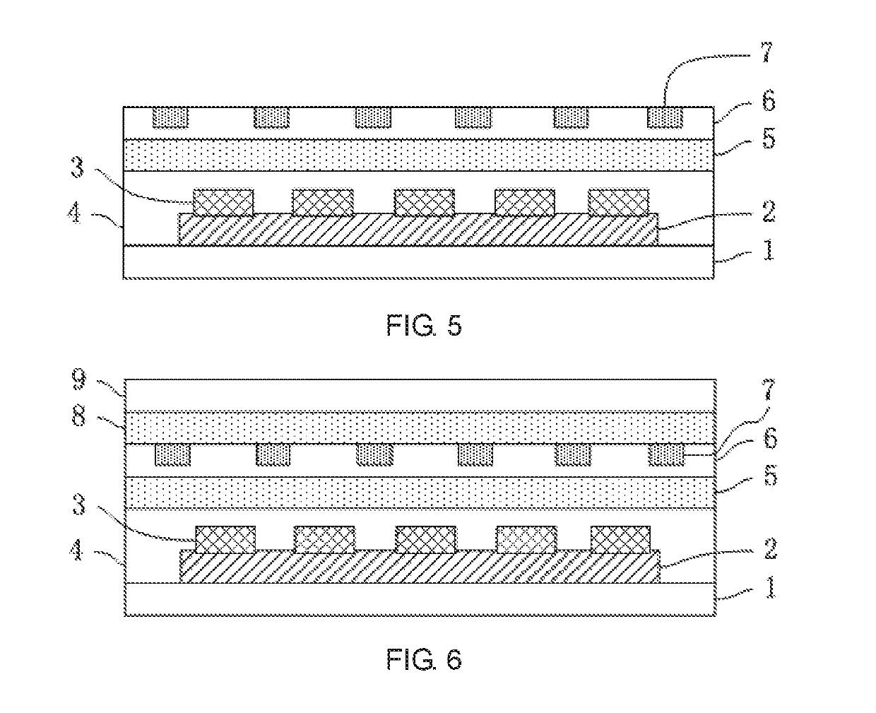
[0056]preparing an organic light emitting diode (OLED) element layer 30 on the thin film transistor layer 2, and preparing a barrier layer and a buffer layer on the glass substrate 1, wherein the barrier layer covers the organic light emitting diode element layer 30; wherein in general, the barrier layer is used to block water vapor and oxygen; here, the barrier layer and the buffer layer constitute a thin film packaging layer;

[0057]preparing a plurality of grooves 61 in the barrier layer, and preparing a water absorbing material layer 7 in the plurality of grooves 61, wherein he...


PUM


Abstract

Provided are an organic light emitting diode display device and a manufacturing method thereof. The method includes: preparing a thin film transistor layer on a glass substrate; preparing an organic light emitting diode element layer on the thin film transistor layer, and preparing a barrier layer and a buffer layer on the glass substrate, wherein the barrier layer covers the OLED element layer; preparing the plurality of grooves in the barrier layer, and preparing a water absorbing material layer in the plurality of grooves. The permeability of water and oxygen is reduced for lowering the risk of breakage of the barrier layer and the buffer layer, and improving the service life of the OLED display device.

Description

CROSS-REFERENCE TO RELATED APPLICATION[0001]This application is a continuing application of PCT Patent Application No. PCT / CN2018 / 089410 entitled “Organic light emitting diode display device and manufacturing method thereof”, filed on May 31, 2018, which claims priority to Chinese Patent Application No. 201810317687.X, filed on Apr. 10, 2018, both of which are hereby incorporated in its entireties by reference.FIELD OF THE INVENTION[0002]The present invention relates to a display field, and more particularly to an organic light emitting diode display device and a manufacturing method thereof.BACKGROUND OF THE INVENTION[0003]In the current field of lighting and display, due to the properties of the OLED (Organic Light-Emitting Diode), such as low start-up voltage, lightness, thinness and self-luminescence, more and more OLEDs are widely studied for the development of lighting products and panel industry to meet the requirements of low energy consumption, light weight and surface ligh...

Claims


Application Information

Patent Timeline
IPC IPC(8): H01L51/52H01L51/56
CPCH01L51/5259H01L51/5253H01L51/56H10K59/12H10K50/846H10K50/8445H10K50/844H10K71/00
Inventor HUANG, HUI
Owner TCL CHINA STAR OPTOELECTRONICS TECH CO LTD
Why Eureka
Try Eureka