Structured light projection system

a light projection and structure technology, applied in the field of optical systems, can solve the problems of affecting the yield, the yield is low, and the production and cost are difficult to increase, so as to achieve the effect of increasing precision and yield

Active Publication Date: 2019-10-17
LIGITEK ELECTRONICS
View PDF0 Cites 3 Cited by
  • Summary
  • Abstract
  • Description
  • Claims
  • Application Information

AI Technical Summary

Benefits of technology

[0004]In view of the abovementioned problem, the Inventor of the disclosure performs research and analysis to the optical area and packaging technology, aiming to design an actual product that meets the requirement mentioned above based on the experience of research and development to related products for years; therefore, the disclosure provides a primary optics design to simply the times of optical axis alignment of optical elements, so as to increase precision and yield of a structured light projection system.

Problems solved by technology

When a plurality of optical lens with different refractive powers combine with one another, optical axes of the optical lenses need to be precisely aligned to avoid the issue of resolution reduction; in addition, each conversion optical lens needs to be arranged and combined in specific intervals, which would consume plenty of production process and precise calibration, making it hard to increase the production and to lower the cost; further, when the plurality of optical lenses in the conversion lens module are stacked, an overall optical effect of the conversion lens module would be affected if the optical axis of one optical lens deviates, and thus affect the yield.
Besides, because each lens on the conversion lens module has an independent optical axis, when one optical lens is stacked on another optical lens, the deviation of the optical axis alignment would accumulate due to the increase of the number of lens layers, making the yield lower, and therefore cannot achieve the effect of thinning.
However, this process is costly and hard to design, which is easy to cause end products to have stability issues.

Method used


Image

  • Structured light projection system
  • Structured light projection system
  • Structured light projection system

Examples


Embodiment Construction

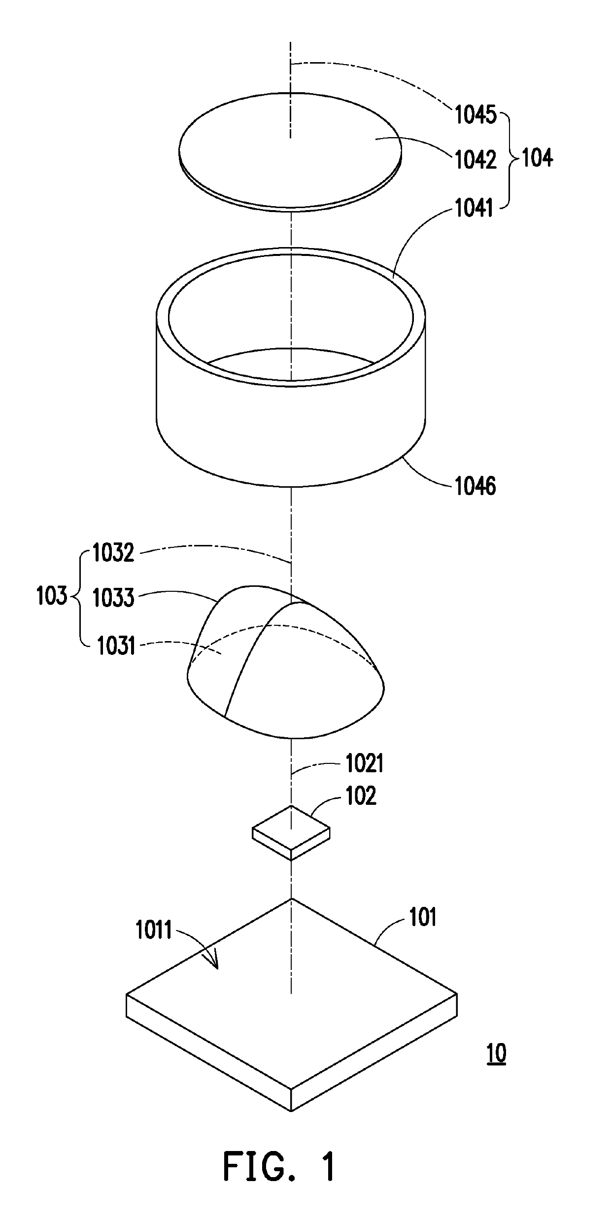
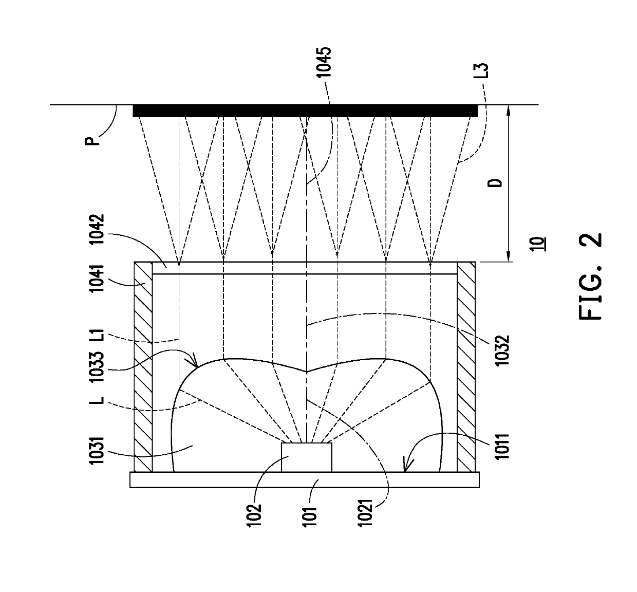
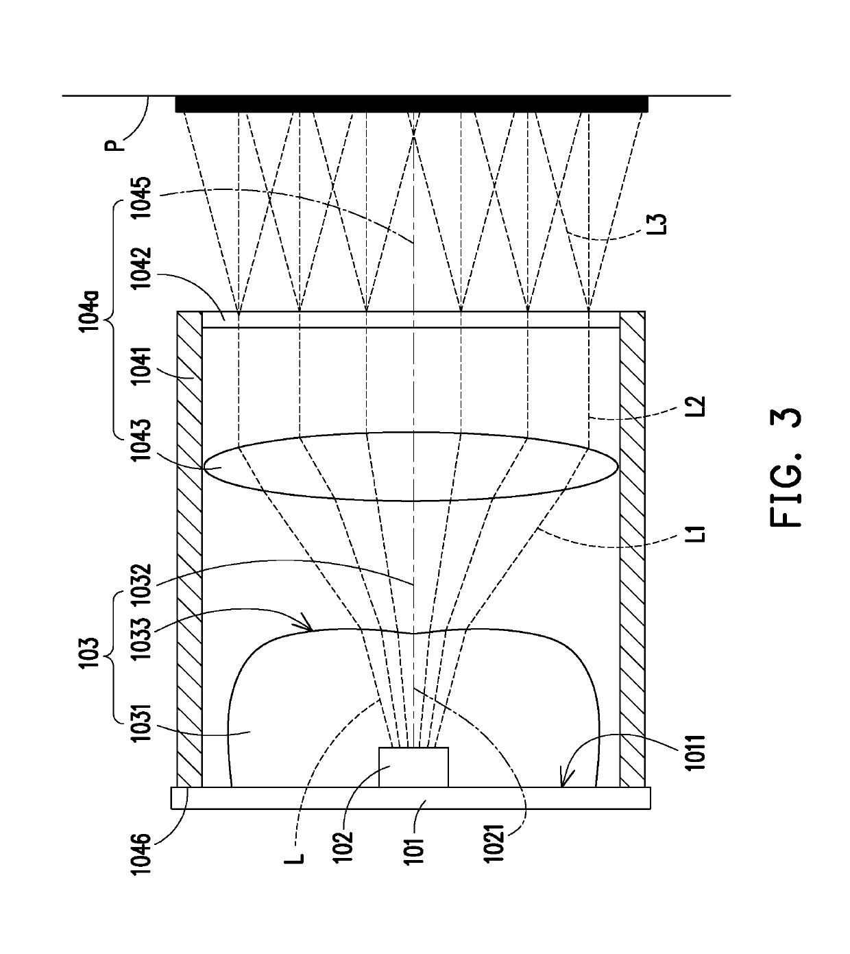
[0018]FIG. 1 is an exploded view of a structured light projection system according to an embodiment of the disclosure. FIG. 2 is a sectional schematic view of the structured light projection system of FIG. 1. Please refer to FIG. 1 and FIG. 2. As shown in the figures, a structured light projection system 10 includes a substrate 101, a semiconductor laser chip 102, a first optical module 103 and a second optical module 104, wherein the substrate 101 may be made of a non-semiconductor material or a semiconductor material. The substrate 101 of the non-semiconductor material may be a metal substrate, a ceramic substrate, or a glass fiber substrate (e.g., FR-4, FR-5, G-10, or G-11) and so on, but is not limited hereto. The substrate 101 has an installation surface 1011. The semiconductor laser chip 102 is electrically disposed on the installation surface 1011 of the substrate 101 and has a first optical axis 1021. The semiconductor laser chip 102 is configured to generate a visible or in...


PUM


Abstract

A structured light projection system including a substrate, a semiconductor laser chip, a first optical module, and a second optical module is provided. The semiconductor laser chip is electrically connected to the substrate. The first optical module is disposed on the substrate. The second optical module is disposed on the first optical module. The deviation rate between optical axes of the optical modules and the semiconductor laser chip and the calibration time thereof are reduced by the first optical module directly packaging the substrate through a primary optics design, so as to increase the yield of the structured light projection.

Description

CROSS-REFERENCE TO RELATED APPLICATION[0001]This application claims the priority benefits of Taiwan application serial no. 107113144, filed on Apr. 16, 2018, and Taiwan application serial no. 108109014, filed on Mar. 14, 2019. The entirety of each of the above-mentioned patent applications is hereby incorporated by reference herein and made a part of this specification.BACKGROUNDTechnical Field[0002]The disclosure relates to an optical system, and in particular to a structured light projection system.Description of Related Art[0003]Along with the prosperous development of optical technology, structured light is further applied in many areas such as 3D contour reproduction, distance measurement, anti-counterfeiting recognition and so on. However, in the exiting technology, the generation method of the structured light is mostly composed of a light emitting module, a lens conversion module, a collimating lens, and a diffractive optical element (DOE). As disclosed by, for example, a pa...

Claims


Application Information

Patent Timeline
Patent Type & Authority Applications(United States)
IPC IPC(8): G03B21/20G02B27/30G02B27/09G03B21/14
CPCG02B27/0944G02B27/30G03B21/142G03B21/2033G02B27/0955G02B27/4205G02B19/0014G02B19/0052G03B21/208G02B27/09
Inventor LEE, HSIAO-WENTUNG, I-HSIN
Owner LIGITEK ELECTRONICS
Why Eureka
Try Eureka