Pixel circuit and driving method thereof, array substrate, and display panel

a pixel circuit and array substrate technology, applied in the field of display technologies, can solve the problems of affecting the driving current of the oled, the threshold voltage of the drive transistor may drift,

Active Publication Date: 2019-11-28
BOE TECH GRP CO LTD +1
View PDF1 Cites 7 Cited by
  • Summary
  • Abstract
  • Description
  • Claims
  • Application Information

AI Technical Summary

Benefits of technology

[0015]In embodiments of the present disclosure, a voltage of the data signal is smaller than a voltage of the reference signal, and the voltage of the reference signal is smaller than a voltage of the first voltage signal from the first voltage signal terminal.
[0016]A second aspect of the present disclosure provides a method for driving the pixel circuit according to the first aspect of the present disclosure. In this method, the reset signal, the second drive signal, and the pixel drive signal may be provided, such that the voltage of the second node is equal to the voltage of the third node, and the drive current of the drive transistor is provided to the third voltage signal terminal via the compensation circuit and the reset circuit to reset the light emitting device. The second drive signal may be provided, such that the voltage of the second node and the voltage of the third node rise to the equal voltage, and the first drive signal may be provided so as to provide the reference signal to the first node, such that a threshold voltage of the drive transistor is a voltage difference between a voltage of the reference signal and a voltage of a first voltage signal from the first voltage signal terminal. The first drive signal may be provided so as to provide the data signal to the first node, and the threshold voltage of the drive transistor may be held to be the voltage difference between the voltage of the reference signal and the voltage of the first voltage signal. Next, the pixel drive signal may be provided, such that the light emitting device emits light based on the drive current of the drive transistor.

Problems solved by technology

Furthermore, as the working time passes and the operating environment changes, the threshold voltage of the drive transistor may drift.
In another aspect, in a display device, different locations for the pixels may also cause different voltage drops (I-R Drops) of a power source, which may affect the driving current of the OLED.

Method used


Image

  • Pixel circuit and driving method thereof, array substrate, and display panel
  • Pixel circuit and driving method thereof, array substrate, and display panel
  • Pixel circuit and driving method thereof, array substrate, and display panel

Examples


Embodiment Construction

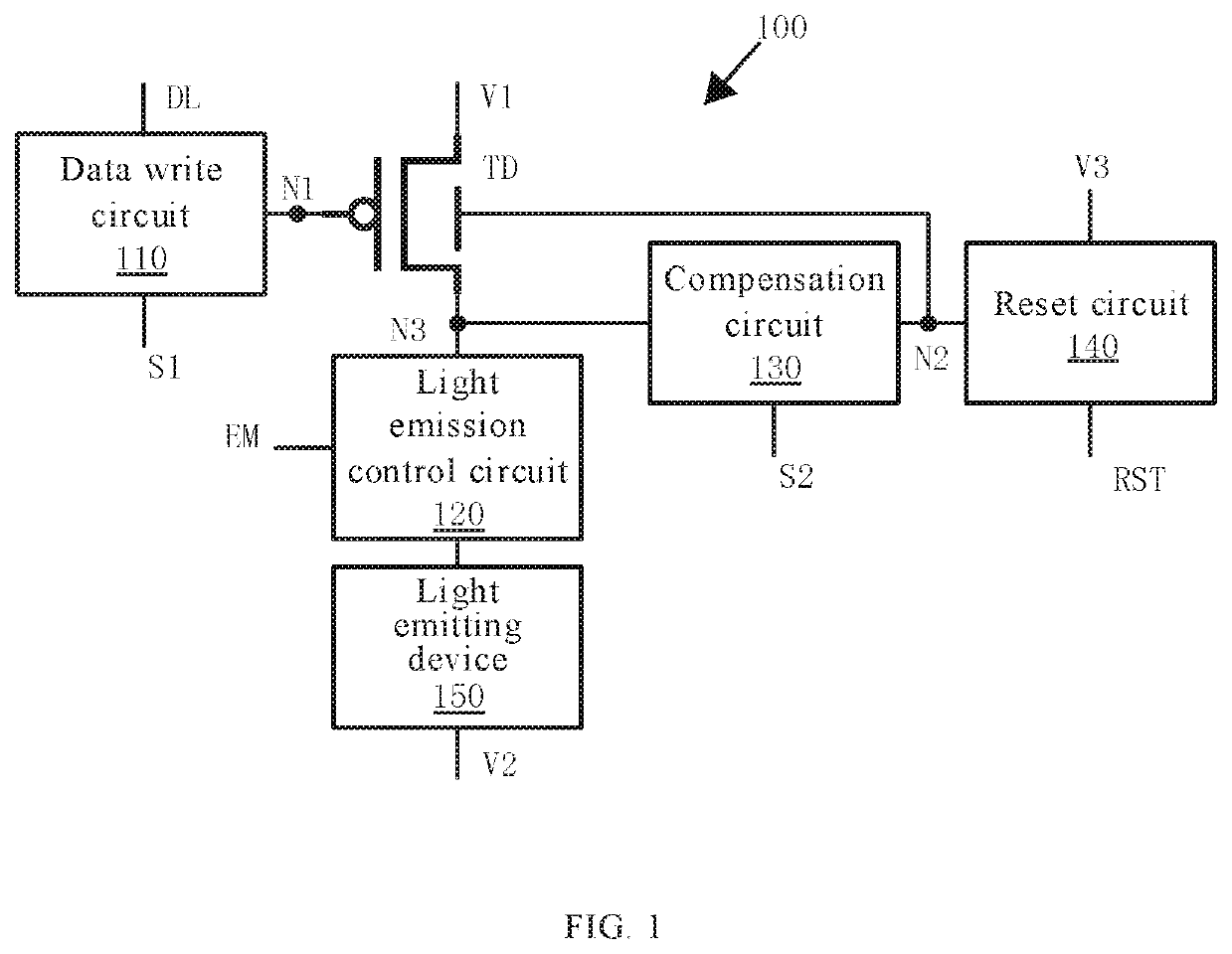
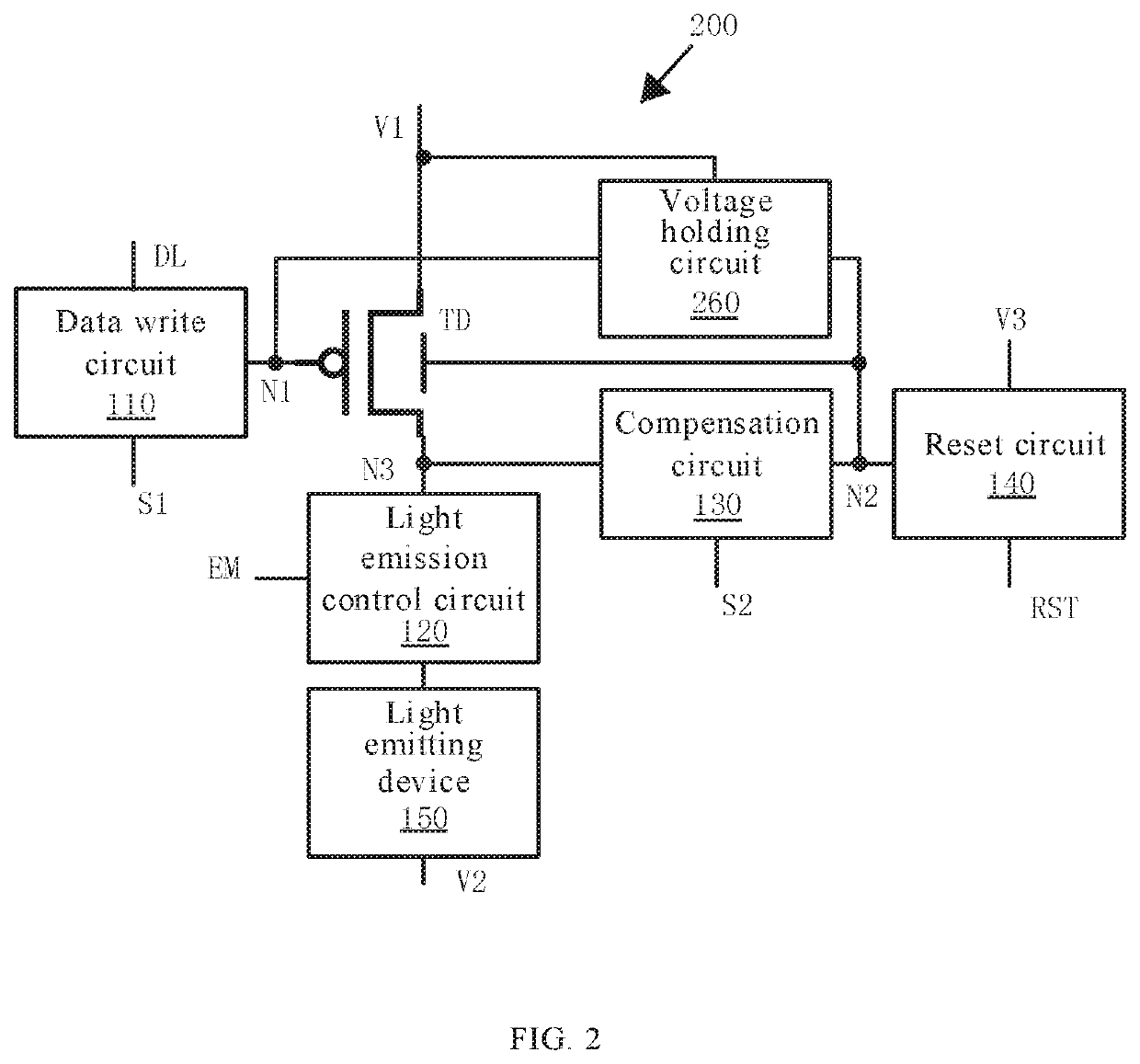
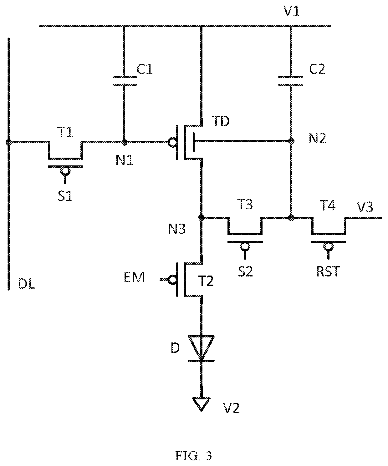
[0027]To make technical solutions and advantages of the embodiments of the present disclosure clearer, the technical solutions in the embodiments of the present disclosure will be described clearly and completely below, in conjunction with the accompanying drawings. Apparently, the described embodiments are merely some but not all of the embodiments of the present disclosure. All other embodiments obtained by those of ordinary skill in the art based on the described embodiments without creative efforts shall fall within the protection scope of the present disclosure.

[0028]In the description of the present disclosure, unless otherwise stated, the term “a plurality of” means two or more than two. The orientation or position relations represented by the terms of “above”, “beneath”, “left”, “right”, “inside”, “outside” and the like are orientation or position relations shown based on the accompanying figures, they are merely for ease of a description of the present disclosure and a simp...


PUM


Abstract

Embodiments of the present disclosure provide a pixel circuit and a drive method thereof, an array substrate, and a display panel. The pixel circuit includes a drive transistor, a data write circuit, a light emission control circuit, a compensation circuit, a reset circuit, and a light emitting device. A first control electrode of the drive transistor is coupled to a first node, a second control electrode of the drive transistor is coupled to a second node, a first electrode of the drive transistor is coupled to a first voltage signal terminal, and a second electrode of the drive transistor is coupled to a third node and may provide a drive current. The light emitting device is coupled between the light emission control circuit and a second voltage signal terminal and may emit light based on the drive current.

Description

CROSS REFERENCE TO RELATED APPLICATIONS[0001]This patent application claims the benefit and priority of Chinese Patent Application No. 201810523030.9 filed on May 28, 2018, the disclosure of which is incorporated by reference herein in its entirety as part of the present application.BACKGROUND[0002]The present disclosure relates to the field of display technologies, and more particularly, to a pixel circuit and a method for driving a pixel circuit, an array substrate, and a display panel.[0003]With the progress of display technologies, a new generation of organic light emitting diode (OLED) display apparatuses have lower manufacturing cost, faster response speed, higher contrast ratio, wider viewing angle, and larger operating temperature range than conventional liquid crystal display (LCD) apparatuses. Furthermore, the OLED display apparatuses do not need backlight units, and have advantages such as bright color and light weight. Therefore, OLED display technologies have become the...

Claims


Application Information

Patent Timeline
Patent Type & Authority Applications(United States)
IPC IPC(8): G09G3/3241G09G3/32
CPCG09G3/3225G09G3/3233G09G2320/0233G09G2300/0819G09G2300/0861G09G2300/0852G09G2320/0223G09G3/32G09G3/3241G09G2320/0204G09G2320/045
Inventor XU, YINGSONG
Owner BOE TECH GRP CO LTD
Why Eureka
Try Eureka