Method for manufacturing gallium nitride substrate using the multi ion implantation

a gallium nitride and multi-ion implantation technology, which is applied in the manufacture of basic electric elements, semiconductor/solid-state devices, electrical equipment, etc., can solve the problems of reducing mechanical strength, unable to form self-supporting substrates, and high fabrication costs of gan substrates or inp substrates. , to achieve the effect of reducing the defect ratio of gallium nitride substrates, low defect density and high quality

Active Publication Date: 2019-12-05
IUCF HYU (IND UNIV COOP FOUND HANYANG UNIV)
View PDF4 Cites 7 Cited by
  • Summary
  • Abstract
  • Description
  • Claims
  • Application Information

AI Technical Summary

Benefits of technology

[0014]Therefore, the present disclosure has been made in view of the above problems, and it is one object of the present disclosure to provide a method of fabricating a gallium nitride substrate characterized by performing first ion implantation at least once to reduce bow of first gallium nitride and then performing second ion implantation to address bowing and cracking, as major factors affecting production yield, of the gallium nitride substrate.
[0015]It is another object of the present disclosure to provide a method of fabricating a gallium nitride substrate having high quality and a low defect density to prevent both a bowing phenomenon and a cracking phenomenon of a gallium nitride substrate.
[0016]It is yet another object of the present disclosure to provide a method of fabricating a gallium nitride substrate characterized by allowing a second gallium nitride, which is used as a seed layer, to grow on a Ga-face of the first gallium nitride to reduce a defect ratio of a gallium nitride substrate.

Problems solved by technology

However, the fabrication costs of the GaN substrate are much higher than those of the GaAs substrate or the InP substrate.
However, when the thickness of GaN films cut out from crystalline GaN bulk is reduced to obtain a larger number of GaN substrates, mechanical strength is decreased, so that self-supporting substrates cannot be formed.
However, bonded substrates fabricated by this method exhibited a problem that a substrate, which is a type different from a GaN thin film, is easily peeled off of the GaN thin film in a process of laminating a semiconductor layer on the GaN thin film.
However, the conventional methods damage crystals inside crystalline GaN bulk, thereby causing appearance deformation such as bowing.
In addition, since it is impossible to recycle crystalline GaN bulk, production costs increase.
However, this method exhibited a problem that multiple layers of a GaN substrate are damaged due to hydrogen ions implanted to both sides of the GaN substrate, and thus, the quality of the GaN substrate is deteriorated.
In addition, the method exhibited a problem that a process is complicated because thermal annealing is performed after ion implantation.

Method used


Image

  • Method for manufacturing gallium nitride substrate using the multi ion implantation
  • Method for manufacturing gallium nitride substrate using the multi ion implantation
  • Method for manufacturing gallium nitride substrate using the multi ion implantation

Examples


Embodiment Construction

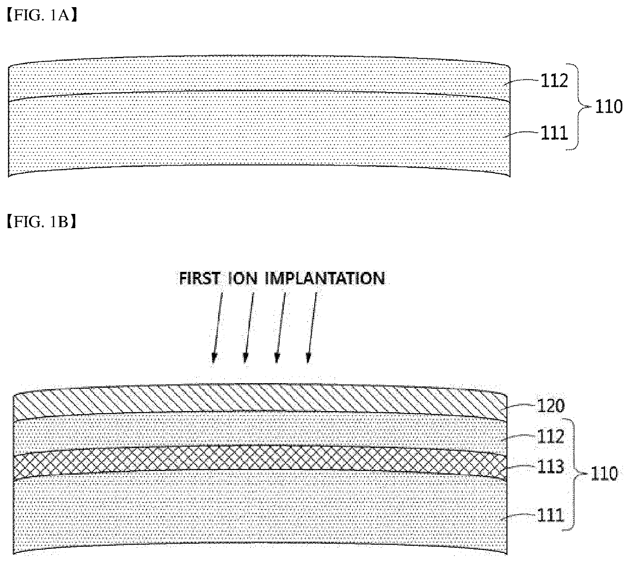
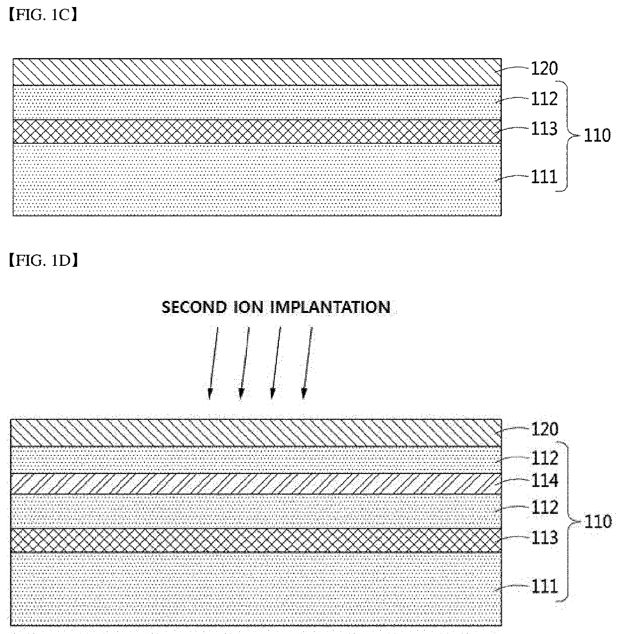
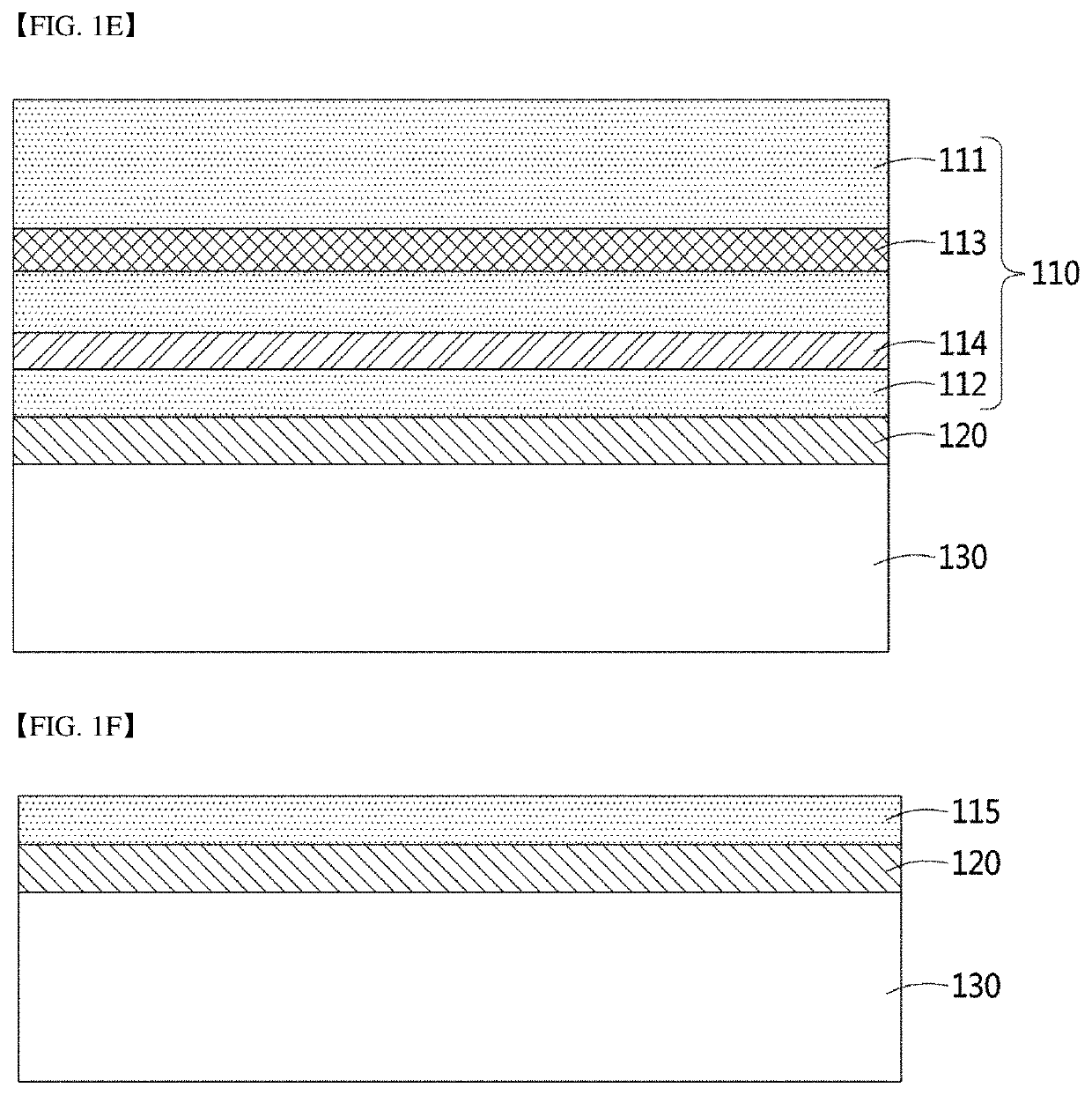
[0039]The present disclosure will now be described more fully with reference to the accompanying drawings and contents disclosed in the drawings. However, the present disclosure should not be construed as limited to the exemplary embodiments described herein.

[0040]The terms used in the present specification are used to explain a specific exemplary embodiment and not to limit the present inventive concept. Thus, the expression of singularity in the present specification includes the expression of plurality unless clearly specified otherwise in context. It will be further understood that the terms “comprise” and / or “comprising”, when used in this specification, specify the presence of stated components, steps, operations, and / or elements, but do not preclude the presence or addition of one or more other components, steps, operations, and / or elements thereof.

[0041]It should not be understood that arbitrary aspects or designs disclosed in “embodiments”, “examples”, “aspects”, etc. used ...


PUM

PropertyMeasurementUnit
thicknessaaaaaaaaaa
thicknessaaaaaaaaaa
depthaaaaaaaaaa

Abstract

Disclosed is a method of fabricating a gallium nitride substrate using a plurality of ion implantation processes. A method of fabricating a gallium nitride substrate using a plurality of ion implantation processes according to an embodiment of the present disclosure includes a step of forming a bonding oxide film on the first gallium nitride; a step of performing first ion implantation for a surface of the first gallium nitride, on which the bonding oxide film is formed, at least once to form a damaged layer, thereby releasing bowing of the first gallium nitride; a step of performing second ion implantation for the surface of the first gallium nitride, on which the bonding oxide film is formed, to form a blister layer; a step of bonding the bonding oxide film of the first gallium nitride to a temporary substrate; a step of separating the first gallium nitride using the blister layer to form a seed layer; and a step of allowing growth of the second gallium nitride using the seed layer to form bulk gallium nitride.

Description

BACKGROUND OF THE DISCLOSUREField of the Disclosure[0001]The present disclosure relates to a method of fabricating a gallium nitride substrate using a plurality of ion implantation processes, and more particularly, to a method of fabricating a gallium nitride substrate having high quality and a low defect density by preventing bowing and cracking of the gallium nitride substrate.Description of the Related Art[0002]The performance and lifespan of semiconductor devices, such as laser diodes and light emitting diodes, are determined by various factors constituting the device, and are particularly affected by a base substrate on which elements are stacked. Several methods of fabricating a high quality semiconductor substrate have been proposed. In addition, interest in III-V compound semiconductor substrates is increasing.[0003]A gallium nitride (GaN) substrate is a typical group III-V compound semiconductor substrate. In addition to a GaAs substrate and an InP substrate, the GaN substr...

Claims


Application Information

Patent Timeline
Patent Type & Authority Applications(United States)
IPC IPC(8): H01L21/02H01L21/265H01L21/768
CPCH01L21/265H01L21/02389H01L21/76871H01L21/2654H01L21/2007
Inventor PARK, JEA GUNSHIM, JAE HYOUNGSHIM, TAE HUN
Owner IUCF HYU (IND UNIV COOP FOUND HANYANG UNIV)
Why Eureka
Try Eureka