Surface acoustic wave device

Inactive Publication Date: 2019-12-05
WISOL
View PDF8 Cites 1 Cited by
  • Summary
  • Abstract
  • Description
  • Claims
  • Application Information

AI Technical Summary

Benefits of technology

[0007]Therefore, the present invention has been made in view of the above problems, and it is an

Problems solved by technology

However, a conventional method of reducing insertion loss is a method of adjusting the distance between electrodes or using a plurality of SAW device

Method used


Image

  • Surface acoustic wave device
  • Surface acoustic wave device
  • Surface acoustic wave device

Examples


first embodiment

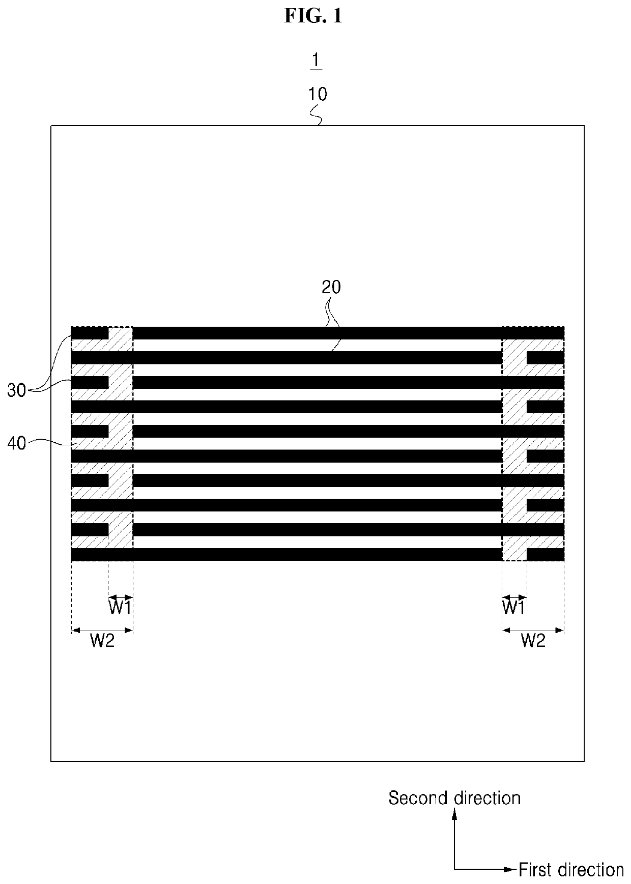
[0032]FIG. 1 is a view showing the top surface of a SAW device 1 according to the present invention.

[0033]Referring to FIG. 1, a SAW device 1 may include a substrate 10, an electrode 20 disposed on the substrate 10, a dummy bar 30 disposed to be adjacent to the electrode 20, and an additional film 40 formed on the dummy bar 30.

[0034]The substrate 10 is formed of a material capable of providing piezoelectric effect, and for example, the substrate 10 may be any one among a silicon substrate, a diamond substrate, a sapphire substrate, a silicon carbide substrate, a LiNbO3 substrate, and a LiTaO3 substrate.

[0035]Next, the electrode 20 may be disposed on the substrate 10 in a first direction. The electrodes 20 may be disposed in plurality at regular intervals in a second direction perpendicular to the first direction and may be divided into an input electrode and an output electrode according to disposition of the dummy bar 30 described below.

[0036]Meanwhile, in the description of the pr...

second embodiment

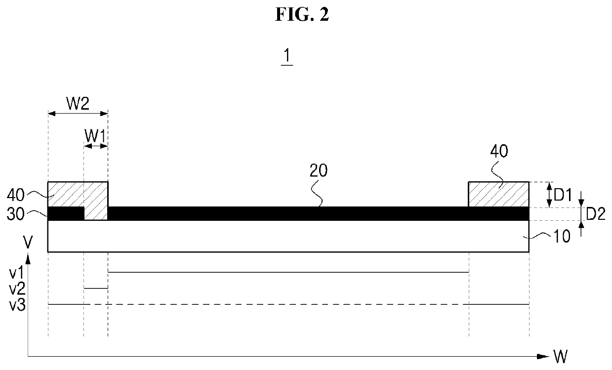
[0054] the additional film 40 may be formed to cover the electrode 20 as much as 0.8 to 1.16λ from the end of the electrode 20 adjacent to the dummy bar 30. Here, 12 means a distance in the second direction from an input electrode and an output electrode of a surface acoustic wave to a next input electrode and a next output electrode, and more preferably, the additional film 40 may be formed to cover the end of the electrode 20 as much as 0.91λ.

[0055]In addition, as the thickness D3 of the additional film 40 formed at the end of the electrode 20 adjacent to the dummy bar 30 is formed to be the same as the thickness D1 of the additional film formed on the predetermined distance W1 between the electrode 20 and the dummy bar 30 and on the dummy bar 30, convenience in the process of manufacturing the SAW device 1 can be enhanced.

[0056]In addition, thickness D1 and D3 of the additional film 40 may larger than the predetermined distance W1 between the dummy bar 30 and the electrode 20.

[00...

third embodiment

[0066]FIG. 6 is a view showing the top surface of a SAW device 1 according to the present invention.

[0067]Referring to FIG. 6, a SAW device 1 according to a third embodiment of the present invention may include a substrate 10, first and second bus bars 25a and 25b disposed on the substrate 10, a plurality of first and second electrodes 20a and 20b formed to be extended from the first and second bus bars 25a and 25b, dummy bars 30 disposed between the first and second bus bars 25a and 25b, an additional film 40 formed on the dummy bars 30, and first and second reflectors 50a and 50b.

[0068]The substrate 10 may be formed of a material capable of providing a piezoelectric effect, like the substrate10 according to a first embodiment of the present invention. For example, the substrate 10 may be any one among a silicon substrate, a diamond substrate, a sapphire substrate, a silicon carbide substrate, a quartz substrate, a LiNbO3 substrate, and a LiTaO3 substrate.

[0069]Next, the first and...


PUM


Abstract

A surface acoustic wave device includes: a substrate; an electrode disposed on the substrate in a first direction; a dummy bar disposed to be spaced apart from the electrode by a predetermined distance in the first direction; and an additional film formed on the dummy bar, wherein the electrode and the dummy bar are disposed in plurality in parallel in a second direction perpendicular to the first direction, and the dummy bars are alternately disposed on a left side or a right side of the electrode to be spaced apart from the electrode by the predetermined distance, and the additional film is formed on the predetermined distance between the electrode and the dummy bar and on the plurality of dummy bars.

Description

CROSS-REFERENCE TO RELATED APPLICATION[0001]The present application claims priority to Korean Patent Application No. 10-2018-0064234, filed Jun. 4, 2018, the disclosure of which is incorporated by reference herein in its entirety.BACKGROUND OF THE INVENTION1. Field of the Invention[0002]The present invention relates to a surface acoustic wave device, and more specifically, to a surface acoustic wave device which can reduce loss of energy.2. Description of Related Art[0003]A surface acoustic wave is an acoustic wave which propagates along the surface of an elastic substrate. Such an acoustic wave is generated from an electrical signal as a result of piezoelectric effect, and if the electric field of the acoustic wave concentrates around the surface of the substrate, the acoustic wave may interact with conductive electrons of another semiconductor, which is put right on the surface of the substrate. A medium which propagates the acoustic wave is a piezoelectric material having high el...

Claims


Application Information

Patent Timeline
IPC IPC(8): H03H9/02
CPCH03H9/02992H03H9/02622H03H9/02574H03H9/25H03H9/64G10K15/00G10K15/04H03H9/02858H03H9/02881H03H9/0004H03H9/6496
Inventor MYEONG, SANG HOONLEE, CHANG MINBAE, SANG KI
Owner WISOL
Why Eureka
Try Eureka