Packaging structure

Active Publication Date: 2019-12-19
NANTONG FUJITSU MICROELECTRONICS
View PDF3 Cites 1 Cited by
  • Summary
  • Abstract
  • Description
  • Claims
  • Application Information

AI Technical Summary

Benefits of technology

The present patent is about a packaging structure for semiconductor chips. It includes conductive connection pillars fixed to the chip's surface, a carrier plate opposite the chip, and solder layers and a second barrier layer between the chip and carrier plate. The technical effects of this structure include improved performance and reliability.

Problems solved by technology

However, performances of a packaging structure formed by an existing flip-chip method are undesirable.

Method used


Image

  • Packaging structure
  • Packaging structure
  • Packaging structure

Examples


Embodiment Construction

[0013]To make the objectives, technical solutions and advantages of the present invention more clear and explicit, the present invention is described in further detail with accompanying drawings and embodiments. It should be understood that the specific exemplary embodiments described herein are only for explaining the present invention and are not intended to limit the present invention.

[0014]Reference will now be made in detail to exemplary embodiments of the present invention, which are illustrated in the accompanying drawings. Wherever possible, the same reference numbers will be used throughout the drawings to refer to the same or like parts.

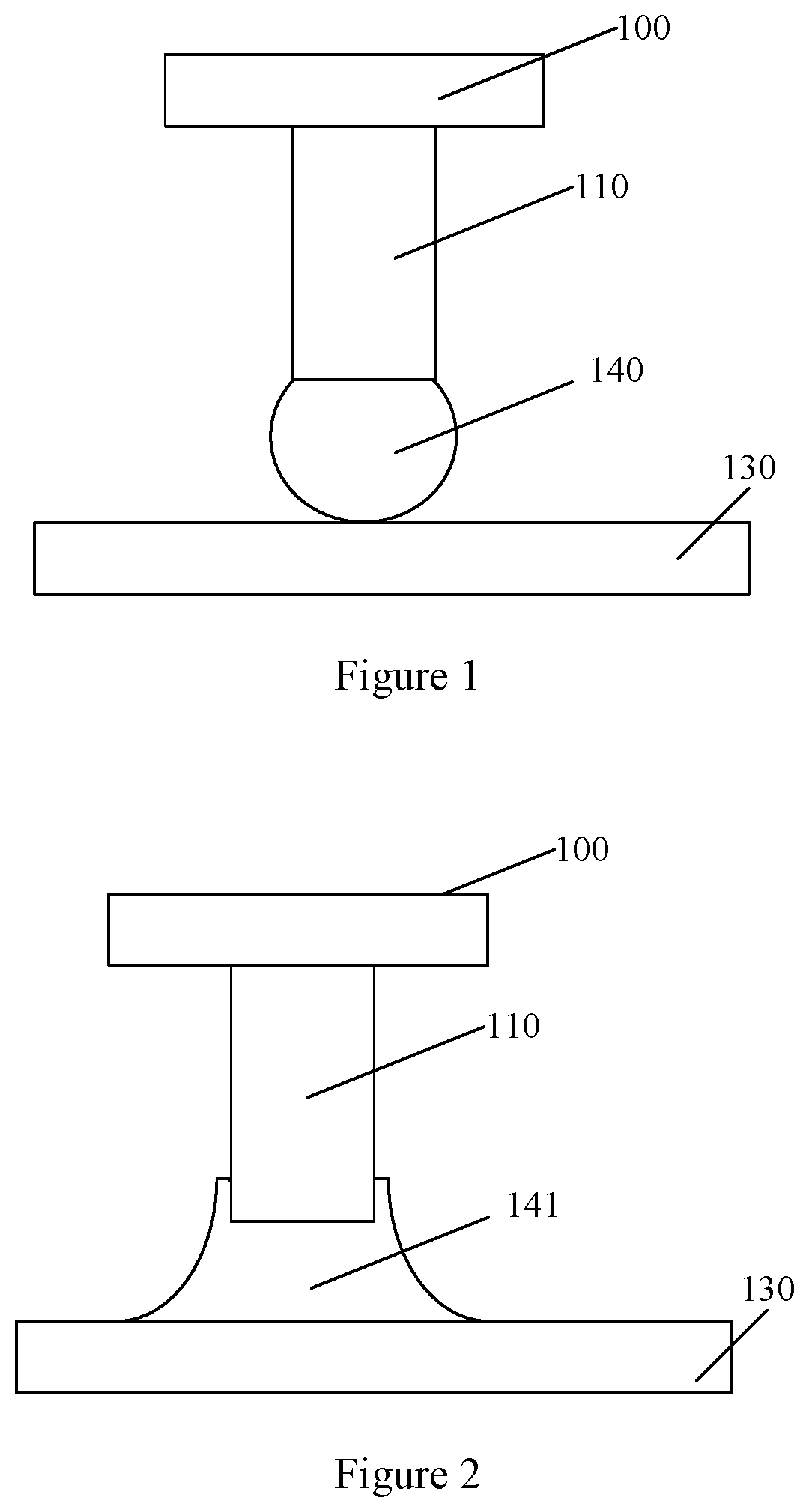
[0015]Performances of a packaging structure formed by an existing flip-chip method are undesirable.

[0016]FIGS. 1 to 2 illustrate structures corresponding to certain stages of an existing flip-chip method. Referring to FIG. 1, a semiconductor chip 100, a conductive connection pillar 110, and a carrier plate 130 are provided. The conductive c...


PUM


Abstract

A packaging structure includes a semiconductor chip and conductive connection pillars. Each of the conductive connection pillars has a first surface and a second surface opposite to the first surface, and the first surfaces of the conductive connection pillars are fixed to a surface of the semiconductor chip. The packaging structure also includes a carrier plate. The carrier plate is disposed opposite to the semiconductor chip. The conductive connection pillars are located between the semiconductor chip and the carrier plate, and the second surfaces face the carrier plate. The packaging structure further includes solder layers located between the carrier plate and the second surfaces, and a barrier layer located on the surface of the carrier plate around the solder layers.

Description

CROSS-REFERENCES TO RELATED APPLICATIONS[0001]This application claims priority of Chinese Patent Application No. 201810614302.6, filed on Jun. 14, 2018, the entire contents of which are hereby incorporated by reference.FIELD OF THE INVENTION[0002]The present disclosure generally relates to the field of packaging and, more particularly, relates to a packaging structure.BACKGROUND[0003]A flip-chip method may be used for chip-interconnection and chip-bonding. International Business Machines Corporation (IBM) developed and used a flip-chip technology more than 50 years ago. However, it is until recently that the flip-chip method became used in packaging high-end devices and in high-density packaging. Currently, the flip-chip packaging technology has been more widely used, with diversified packaging forms and increased demands.[0004]However, performances of a packaging structure formed by an existing flip-chip method are undesirable. The disclosed methods and structures are directed to s...

Claims


Application Information

Patent Timeline
IPC IPC(8): H01L23/31H01L23/00H01L23/498H01L23/48H01L21/56
CPCH01L23/3114H01L24/33H01L24/17H01L21/56H01L23/3128H01L23/49816H01L23/481H01L24/73H01L23/49H01L23/3121H01L21/4853H01L23/49811H01L23/49541H01L23/4952H01L2224/81191H01L2224/81411H01L2224/81416H01L2224/16237H01L2224/10175H01L2224/81193H01L2224/13111H01L2224/13116H01L2224/81815H01L2224/13005H01L2224/16245H01L24/81H01L24/13H01L24/16H01L2224/13147H01L2924/3841H01L2924/014H01L2924/01047H01L2924/00014H01L2924/01029H01L2924/01082H01L2924/0105H01L2924/206
Inventor SHI, LEI
Owner NANTONG FUJITSU MICROELECTRONICS
Why Eureka
Try Eureka