
Method for Producing Polycrystalline Silicon Processed Article

a polycrystalline silicon and processing article technology, applied in silicon compounds, chemistry apparatus and processes, inorganic chemistry, etc., can solve the problems of reactor and the polycrystalline silicon rod may be contaminated, and the carbon contamination of the polycrystalline silicon rod surface can be effectively avoided, and the polycrystalline silicon rod surface can be obtained stably. high-quality polycrystalline silicon processing articles

Active Publication Date: 2020-01-09
TOKUYAMA CORP
View PDF0 Cites 1 Cited by
  • Summary
  • Abstract
  • Description
  • Claims
  • Application Information

AI Technical Summary

Benefits of technology

The present invention provides a novel method for producing a polycrystalline silicon processed article that prevents carbon contamination on the surface of the polycrystalline silicon rod caused by a carbon member at the end of the polycrystalline silicon rod during handling. By handling the polycrystalline silicon rod and the carbon member separately, the risk of carbon contamination can be effectively avoided, resulting in a highly clean polycrystalline silicon processed article.

Problems solved by technology

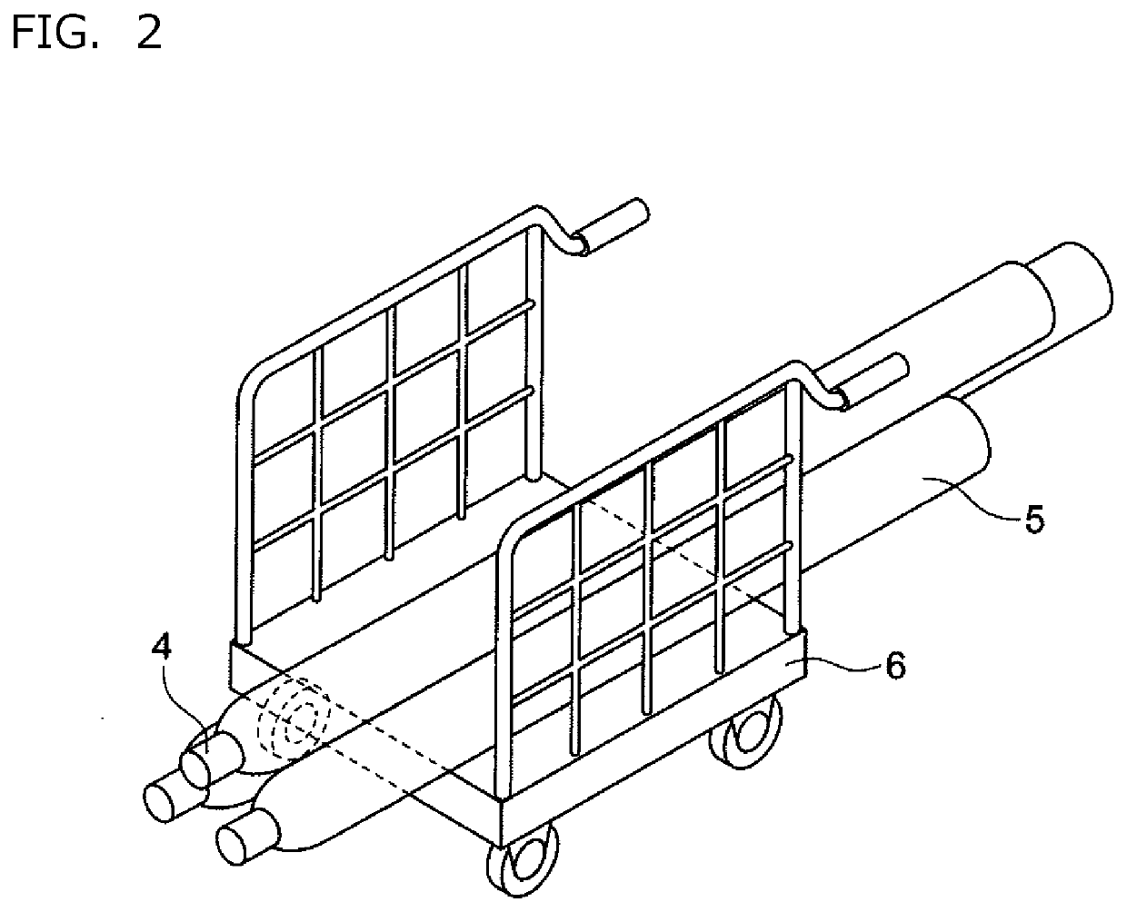
As a result, it was found that the carbon member was a major cause of contamination when the polycrystalline silicon rod is taken out from the reactor or when it is carried by the push cart.
By carrying the polycrystalline silicon rod in such state using the push cart, a fragment of the carbon member which fell off contacts the surface of the polycrystalline silicon rod while inside the plastic bag, and there is a possibility of carbon contamination taking place.
Also, the polycrystalline silicon rod may be placed inside the plastic bag after the carbon member at the end of the polycrystalline silicon rod is removed while inside the reactor, however part of carbon scatters when the carbon member is removed, thus the reactor and the polycrystalline silicon rod may be contaminated.

Method used


Image

  • Method for Producing Polycrystalline Silicon Processed Article
  • Method for Producing Polycrystalline Silicon Processed Article
  • Method for Producing Polycrystalline Silicon Processed Article

Examples


Embodiment Construction

[0024]Hereinafter, an embodiment of the present invention is described in detail. First, terms used in the present specification are explained in below.

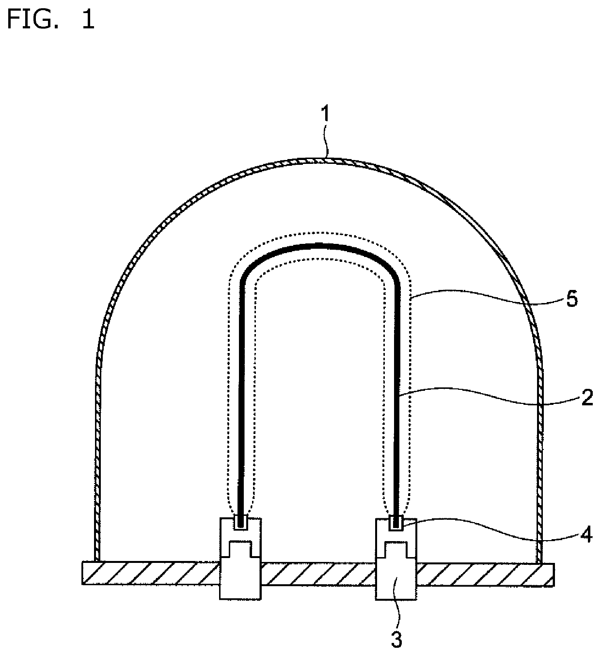
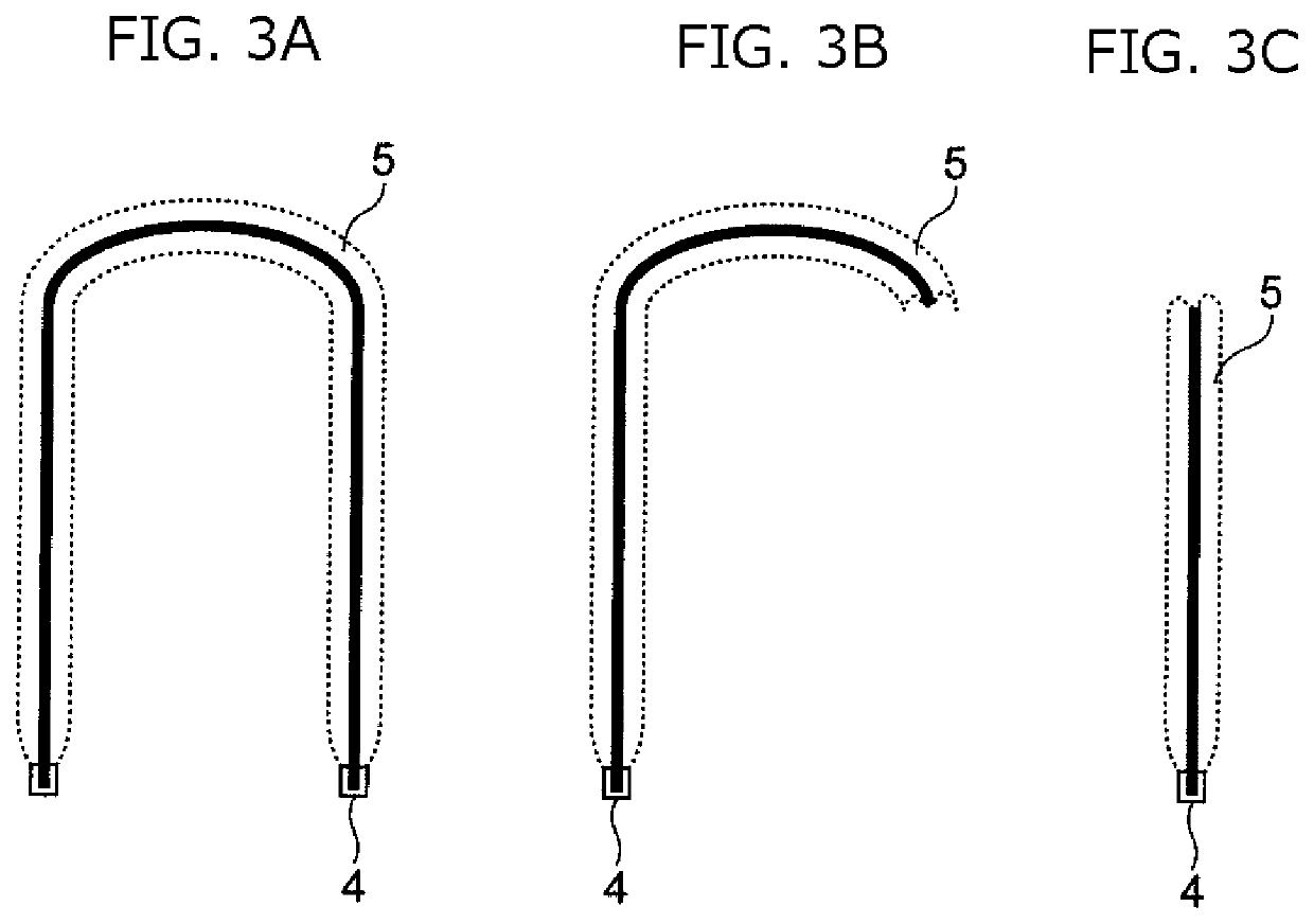
[0025]A polycrystalline silicon rod is a columnar shape object of polycrystalline silicon obtained by using Siemens reactor as shown in FIG. 1 and it is made of the polycrystalline silicon deposited to a surface of a silicon core wire. According to Siemens method, a polycrystalline silicon rod is obtained as inverted U shape, but the polycrystalline silicon rod according to the present invention may be L shape of which a part of inverted U shape is lost, or it may be a rod shape.

[0026]Also, an end of the polycrystalline silicon rod is a part which contacts with an upper end part of the carbon member. This end part and nearby area of the end part may be referred as “a lower part” of the polycrystalline silicon rod.

[0027]An upper part of the polycrystalline silicon rod refers to a part besides the lower part, and it corresponds to a pa...


PUM


Abstract

A method for producing a polycrystalline silicon processed article includes removing a polycrystalline silicon rod, obtained by precipitating polycrystalline silicon on a silicon core wire held by a carbon member connected to an electrode in a reactor by the Siemens method, in a state in which the carbon member is included at the end portion thereof and processing the polycrystalline silicon rod. The polycrystalline silicon rod is detached from the electrode and the carbon member present on the end portion of the polycrystalline silicon rod is covered using a covering material until the processing, whereby the polycrystalline silicon rod and the carbon member are handled in a separated state.

Description

TECHNICAL FIELD[0001]The present invention relates to a novel method for producing a polycrystalline silicon processed article. Specifically, the present invention provides the novel method for producing the polycrystalline silicon processed article including a step of preventing a carbon contamination of a surface of a polycrystalline silicon rod caused by a carbon member which is provided at an end of the polycrystalline silicon rod when handling the polycrystalline silicon rod obtained by Siemens method.BACKGROUND OF THE INVENTION[0002]A polycrystalline silicon used as a raw material of a semiconductor or a solar battery wafer is obtained as a polycrystalline silicon rod 5 usually by Siemens method in which a silicon core wire 2 having inverted U shape, which becomes a seed rod, is held by a carbon member 4 connected to an electrode 3 in a reactor 1 as shown in FIG. 1 and a polycrystalline silicon is deposited to a surface of the silicon core wire. Then, the polycrystalline silic...

Claims


Application Information

Patent Timeline
IPC IPC(8): C01B33/035
CPCC01B33/035
Inventor AKIYOSHI, AYAO
Owner TOKUYAMA CORP
Learn More