

Silicon wafer heat treatment method
- Summary
- Abstract
- Description
- Claims
- Application Information
AI Technical Summary
Benefits of technology
Problems solved by technology
Method used
Image

Examples
examples
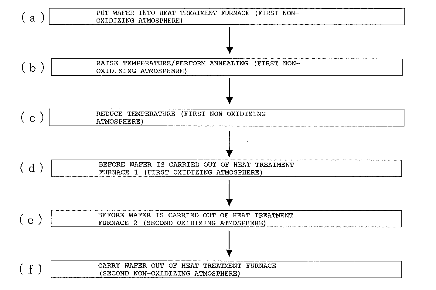
[0043]Hereinafter, the present invention will be described more specifically with Example and Comparative Example, but the present invention is not limited by these examples.
example
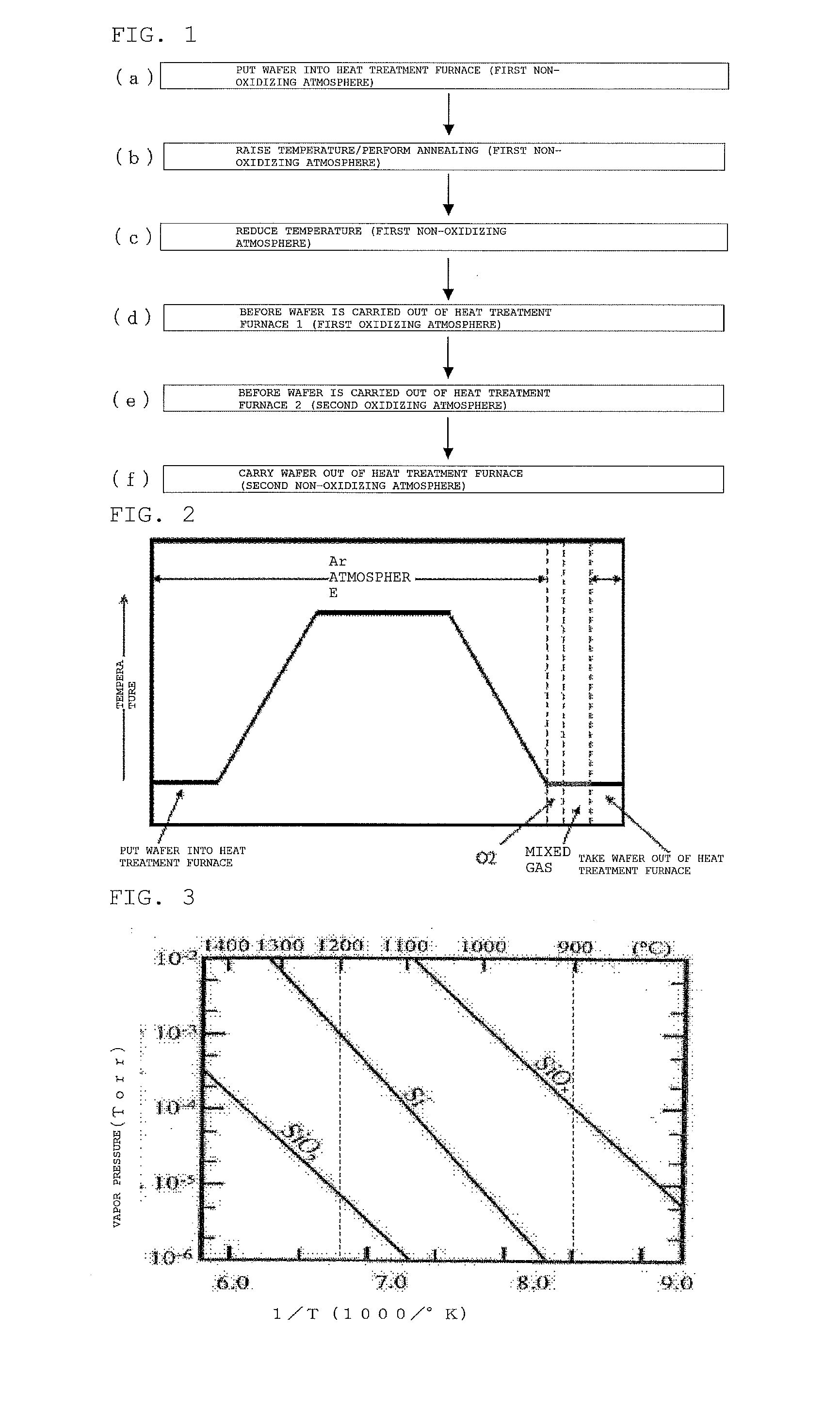
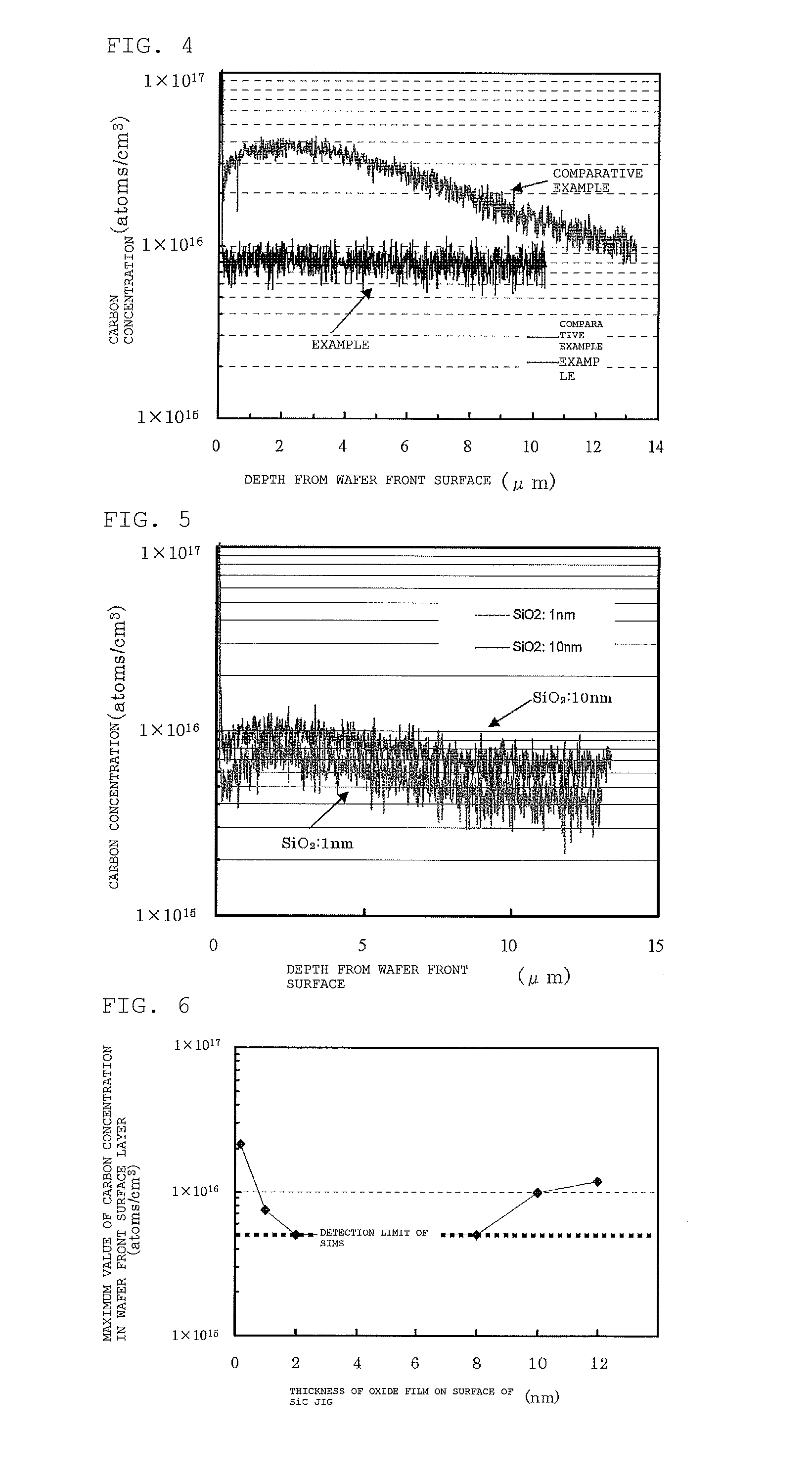
[0044]A nitrogen-doped P-type silicon wafer having a diameter of 300 mm (specific resistance: 8 to 12 acm, oxygen concentration: 15 ppma (JEIDA (Japan Electronic Industry Development Association Standards)), nitrogen concentration 5×10¹³ atoms / cm3) was prepared. After pre-heat treatment cleaning was performed on this wafer, the wafer was placed on the SiC jig and was put into the heat treatment furnace at 700° C. The temperature was raised to 1200° C., heat treatment by which holding was performed for 1 hour was performed, and the temperature was reduced to 700° C. The temperature rise, holding, and temperature reduction were performed in a 100% argon atmosphere. Then, the 100% argon atmosphere was switched to a 100% oxygen atmosphere, oxygen was supplied for 30 seconds, the atmosphere was switched to the 100% argon atmosphere after purging was performed in a 0.6% oxygen atmosphere for about 10 minutes, and the wafer was taken out thereof in the 100% argon atmosphere.
[0045]By so doi...
PUM
 Abstract
Description
Claims
Application Information