Silicon wafer heat treatment method

a technology of silicon wafers and heat treatment methods, applied in the direction of crystal growth process, polycrystalline material growth, after-treatment details, etc., can solve the problems of difficult suppression of reliably carbon contamination, leakage current generation, and difficult to suppress carbon contamination, so as to prevent the release of carbon, eliminate the cause of the device operating failure, and prevent the effect of carbon contamination

Active Publication Date: 2017-07-18
SHIN-ETSU HANDOTAI CO LTD
View PDF17 Cites 0 Cited by
  • Summary
  • Abstract
  • Description
  • Claims
  • Application Information

AI Technical Summary

Benefits of technology

[0013]With the silicon wafer heat treatment method of the present invention, it is possible to prevent release of carbon from the SiC jig itself. As a result, it is possible to prevent carbon contamination of the silicon wafer. This makes it possible to eliminate the cause of a device operating failure. Moreover, since a thick oxide film is not formed on the front surface of the silicon wafer, there is no need for removal of the oxide film and a polishing process.

Problems solved by technology

The silicon wafer contaminated by carbon forms a defect in a device process and causes a leakage current or the like.
Moreover, contaminated carbon becomes a carbon donor and becomes a cause of the generation of a Vth (threshold voltage) shift of a device and a device operating failure.
However, although. this method is expected to have an effect to some extent as the measures against carbon contamination, the amount of carbon coming out from the SiC jig due to high-temperature oxidation is large and the above measures are not measures to suppress carbon generation itself from the source of carbon contamination, and therefore it is difficult to suppress reliably carbon contamination only with the above measures.
Furthermore, since the oxide film is formed at a high temperature, oxygen is implanted into a wafer surface layer and the defect size of a defect which has not been eliminated in a surface layer portion is increased due to a supply of oxygen, which becomes a cause of degradation of electrical characteristics.

Method used


Image

  • Silicon wafer heat treatment method
  • Silicon wafer heat treatment method
  • Silicon wafer heat treatment method

Examples


examples

[0043]Hereinafter, the present invention will be described more specifically with Example and Comparative Example, but the present invention is not limited by these examples.

example

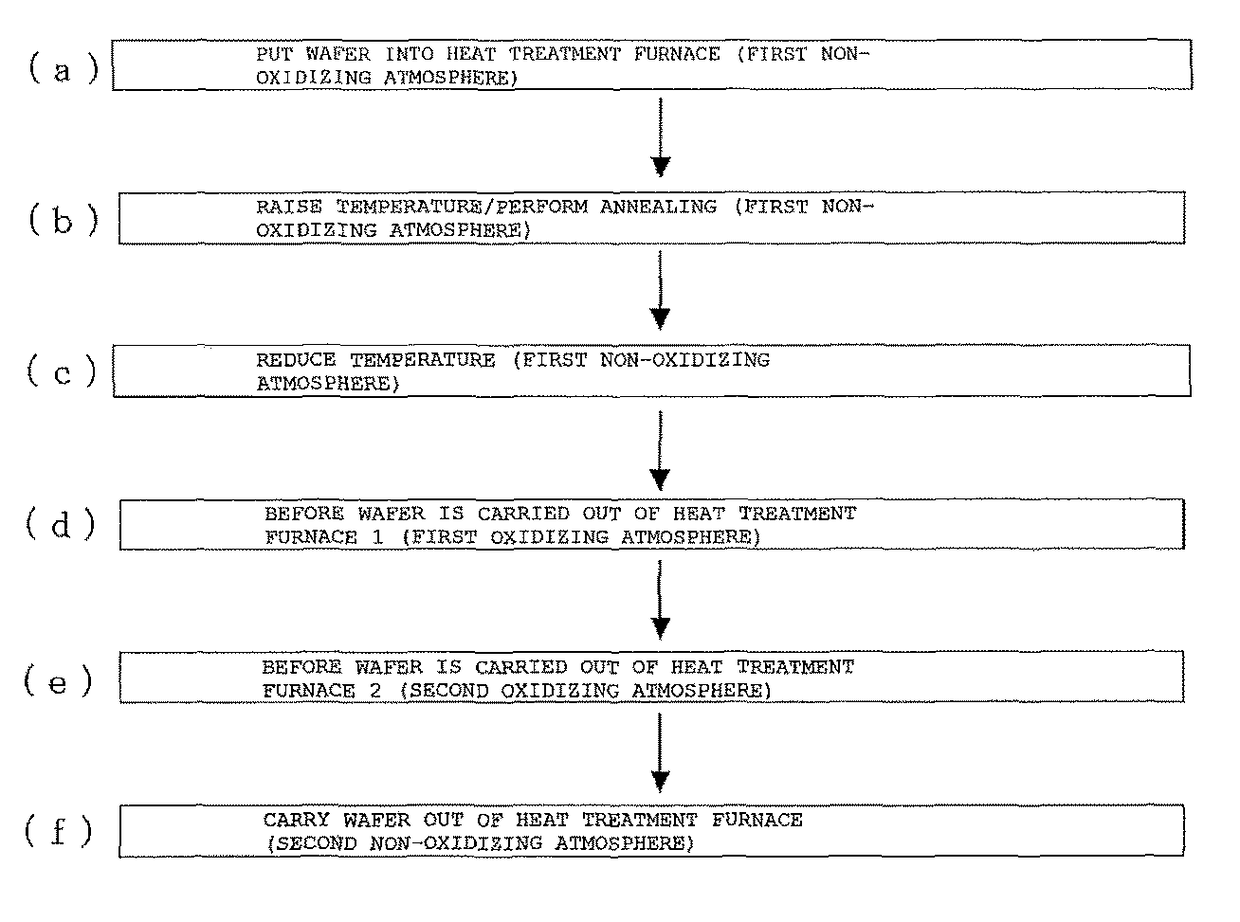
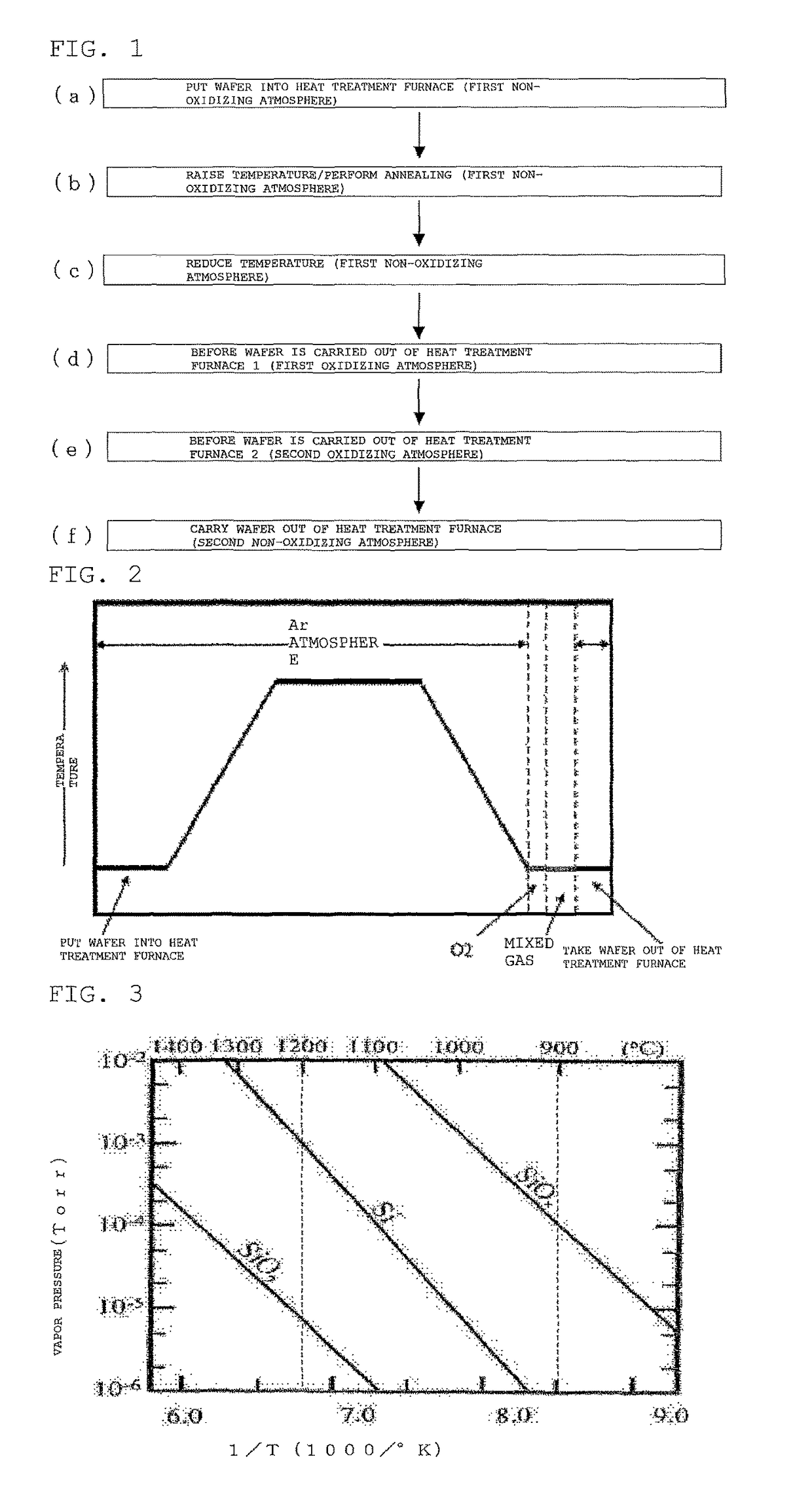
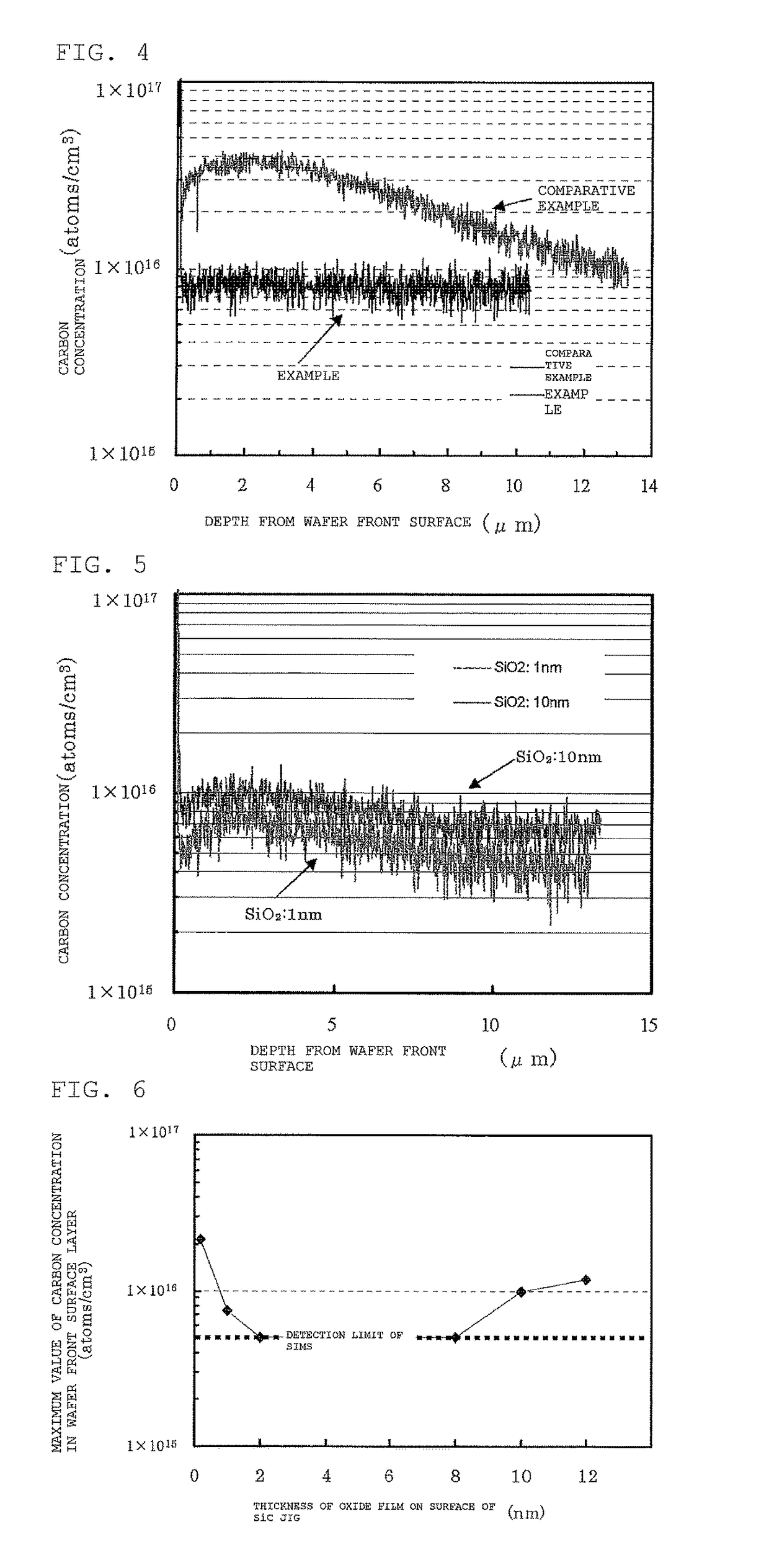
[0044]A nitrogen-doped P-type silicon wafer having a diameter of 300 mm (specific resistance: 8 to 12 acm, oxygen concentration: 15 ppma (JEIDA (Japan Electronic Industry Development Association Standards)), nitrogen concentration 5×10¹³ atoms / cm3) was prepared. After pre-heat treatment cleaning was performed on this wafer, the wafer was placed on the SiC jig and was put into the heat treatment furnace at 700° C. The temperature was raised to 1200° C., heat treatment by which holding was performed for 1 hour was performed, and the temperature was reduced to 700° C. The temperature rise, holding, and temperature reduction were performed in a 100% argon atmosphere. Then, the 100% argon atmosphere was switched to a 100% oxygen atmosphere, oxygen was supplied for 30 seconds, the atmosphere was switched to the 100% argon atmosphere after purging was performed in a 0.6% oxygen atmosphere for about 10 minutes, and the wafer was taken out thereof in the 100% argon atmosphere.

[0045]By so doi...


PUM

PropertyMeasurementUnit
thicknessaaaaaaaaaa
temperatureaaaaaaaaaa

Abstract

A silicon wafer heat treatment method includes: placing a silicon wafer on a SiC jig and into a heat treatment furnace; performing heat treatment on the silicon wafer in the heat treatment furnace in a first non-oxidizing atmosphere; reducing the temperature; and carrying the silicon wafer out of the heat treatment furnace. In the heat reduction step, after the temperature is reduced to the temperature at which the silicon wafer can be carried out of the heat treatment furnace, the first non-oxidizing atmosphere is switched to an atmosphere containing oxygen, an oxide film having a thickness of 1 to 10 nm is formed on the surface of the SiC jig in the atmosphere containing oxygen, and the atmosphere containing oxygen is then switched to a second non-oxidizing atmosphere. A silicon wafer heat treatment method can prevent carbon contamination from a jig and an environment during a heat treatment process.

Description

TECHNICAL FIELD[0001]The present invention relates to silicon wafer heat treatment methods.BACKGROUND ART[0002]By performing heat treatment on surface layer defects (COPs) of a silicon wafer in a non-oxidizing atmosphere, the surface layer COPs are eliminated. In the case of high-temperature heat treatment, a SiC jig is often used, and an environment in which a silicon single crystal wafer (hereinafter referred to simply as a silicon wafer) subjected to heat treatment is taken out of something contains oxygen and a carbonation product, which become a source of carbon contamination of the silicon wafer. The silicon wafer contaminated by carbon forms a defect in a device process and causes a leakage current or the like. Moreover, contaminated carbon becomes a carbon donor and becomes a cause of the generation of a Vth (threshold voltage) shift of a device and a device operating failure.[0003]Thus, forming an oxide layer on a silicon wafer as the measures against carbon contamination o...

Claims


Application Information

Patent Timeline
Patent Type & Authority Patents(United States)
IPC IPC(8): C30B33/02C30B29/06H01L21/324C30B1/04
CPCC30B1/04C30B29/06C30B33/02H01L21/324H01L21/0223H01L21/164
Inventor QU, WEI FENGTAHARA, FUMIO
Owner SHIN-ETSU HANDOTAI CO LTD
Why Eureka
Try Eureka