Process for manufacturing microelectromechanical devices, in particular electroacoustic modules

a technology of electroacoustic modules and manufacturing processes, which is applied in the field of electroacoustic modules, can solve the problems of low flexibility of the process and the inability of the manufacturing process to test the asics,

Active Publication Date: 2020-01-23
STMICROELECTRONICS SRL
View PDF0 Cites 1 Cited by
  • Summary
  • Abstract
  • Description
  • Claims
  • Application Information

AI Technical Summary

Problems solved by technology

However, this is difficult because of the high number of transducers (of the order of thousands) that are typically used.
This process, however, is characterized by a low flexibility, since it envisages adoptin

Method used


Image

  • Process for manufacturing microelectromechanical devices, in particular electroacoustic modules
  • Process for manufacturing microelectromechanical devices, in particular electroacoustic modules
  • Process for manufacturing microelectromechanical devices, in particular electroacoustic modules

Examples


Embodiment Construction

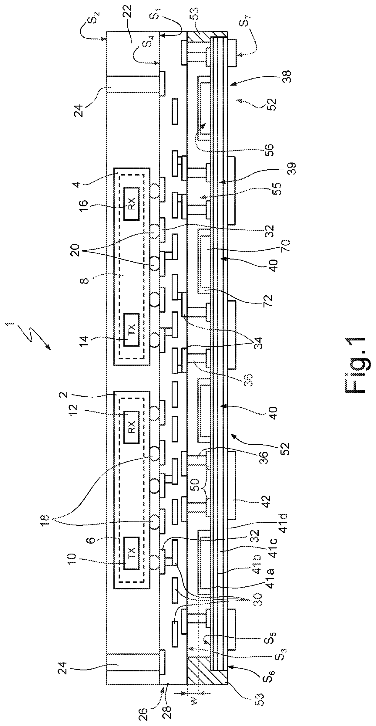
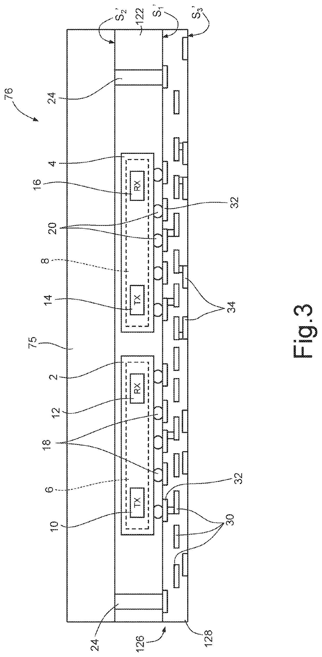
[0018]FIG. 1 shows an electroacoustic module 1, which comprises a first die 2 and a second die 4, formed inside which are, respectively, a first integrated circuit 6 and a second integrated circuit 8, formed, for example, by ASICs of a known type. Each of the first and second integrated circuits 6, 8 comprises a respective transmission circuit and a respective reception circuit, which are designated, respectively, by 10 and 12, in the case of the first integrated circuit 6, and by 14 and 16, in the case of the second integrated circuit 8.

[0019]Albeit not shown in detail, in each of the first and second integrated circuits 6, 8, the corresponding transmission and reception circuits are electrically connected to a corresponding plurality of metal bumps, designated, respectively, by 18 and 20 and also known as “microbumps”. Once again in a way in itself known, the bumps 18, 20 are electrically connected to the so-called last-level metallizations of the corresponding dice.

[0020]The elec...


PUM

PropertyMeasurementUnit
Dielectric polarization enthalpyaaaaaaaaaa
Electrical conductoraaaaaaaaaa
Deformation enthalpyaaaaaaaaaa

Abstract

A process for manufacturing MEMS devices, includes forming a first assembly, which comprises: a dielectric region; a redistribution region; and a plurality of unit portions. Each unit portion of the first assembly includes: a die arranged in the dielectric region; and a plurality of first and second connection elements, which extend to opposite faces of the redistribution region and are connected together by paths that extend in the redistribution region, the first connection elements being coupled to the die. The process further includes: forming a second assembly which comprises a plurality of respective unit portions, each of which includes a semiconductor portion and third connection elements; mechanically coupling the first and second assemblies so as to connect the third connection elements to corresponding second connection elements; and then removing at least part of the semiconductor portion of each unit portion of the second assembly, thus forming corresponding membranes.

Description

BACKGROUNDTechnical Field[0001]The present disclosure relates to a process for manufacturing microelectromechanical systems (MEMS) devices, and in particular electroacoustic modules.Description of the Related Art[0002]As is known, numerous ultrasonic sensors are today available, which are adapted to transmit and receive acoustic waves with frequencies higher than 20 kHz. Typically, an ultrasonic sensor comprises, in addition to a transducer of an electroacoustic type, a circuitry adapted to drive the transducer, as well as to amplify the electrical signals generated by the transducer itself following upon reception of echo acoustic signals. The transducer hence functions both as acoustic emitter and as acoustic receiver, in different periods of time.[0003]If we designate as “stimulus acoustic signals” and as “response acoustic signals”, respectively, the acoustic signals (or beams) transmitted by the transducer and the acoustic signals (or beams) that impinge on the transducer, for ...

Claims


Application Information

Patent Timeline
IPC IPC(8): B81B7/00B81C1/00
CPCB81C2203/035H01L29/66B81B7/007B81C1/0023B81B7/008B81C1/00301B81C1/00325B81C1/00333B81B7/0006B81C2203/019B81B2201/0292B81B2207/09B81C1/00238B81C2203/0792B81B2201/0271
Inventor QUAGLIA, FABIOFERRERA, MARCODEL SARTO, MARCO
Owner STMICROELECTRONICS SRL
Why Eureka
Try Eureka