Methods of improving efficiency of displays using quantum dots with integrated optical elements

a technology of quantum dots and optical elements, applied in the field of display devices, can solve the problemscompromising display quality or performance, and affecting the performance of display devices, etc., and achieve the effect of reducing display device thickness, sacrificing display quality or performance, and reducing consumer demand for thin display devices

Active Publication Date: 2020-01-30
SHOEI CHEM IND CO LTD
View PDF8 Cites 5 Cited by
  • Summary
  • Abstract
  • Description
  • Claims
  • Application Information

AI Technical Summary

Benefits of technology

[0004]Consumer demand for thin display devices is surging. However, it may be difficult for manufacturers to achieve reductions in display device thickness without sacrificing display quality or performance. For example, generally a display device may require an optical film (also referred to as an optical feature film) to achieve sufficient quality brightness and optical characteristics. Reducing the dimensions of an optical film may affect the capability of the film to direct light off-axis or otherwise enhance optical features of display light. This disclosure provides a display device that maintains expected quality and performance while eliminating or combining layers and achieving desirable reductions in overall device thickness.
[0007]According to some embodiments, a display device is provided that can include a quantum dot layer on a surface of a light guide plate without an intervening layer. The quantum dot film can be provided having a population of embedded microspheres to achieve optical effects without a separate optical film. In some embodiments, the microspheres can have sizes distributed irregularly to improve the overall thickness uniformity of the quantum dot film.

Problems solved by technology

Consumer demand for thin display devices is surging.
However, it may be difficult for manufacturers to achieve reductions in display device thickness without sacrificing display quality or performance.

Method used


Image

  • Methods of improving efficiency of displays using quantum dots with integrated optical elements
  • Methods of improving efficiency of displays using quantum dots with integrated optical elements
  • Methods of improving efficiency of displays using quantum dots with integrated optical elements

Examples


Embodiment Construction

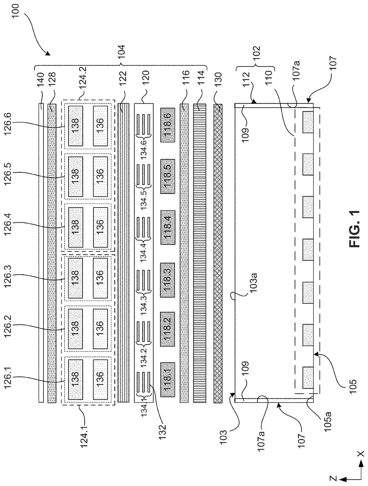
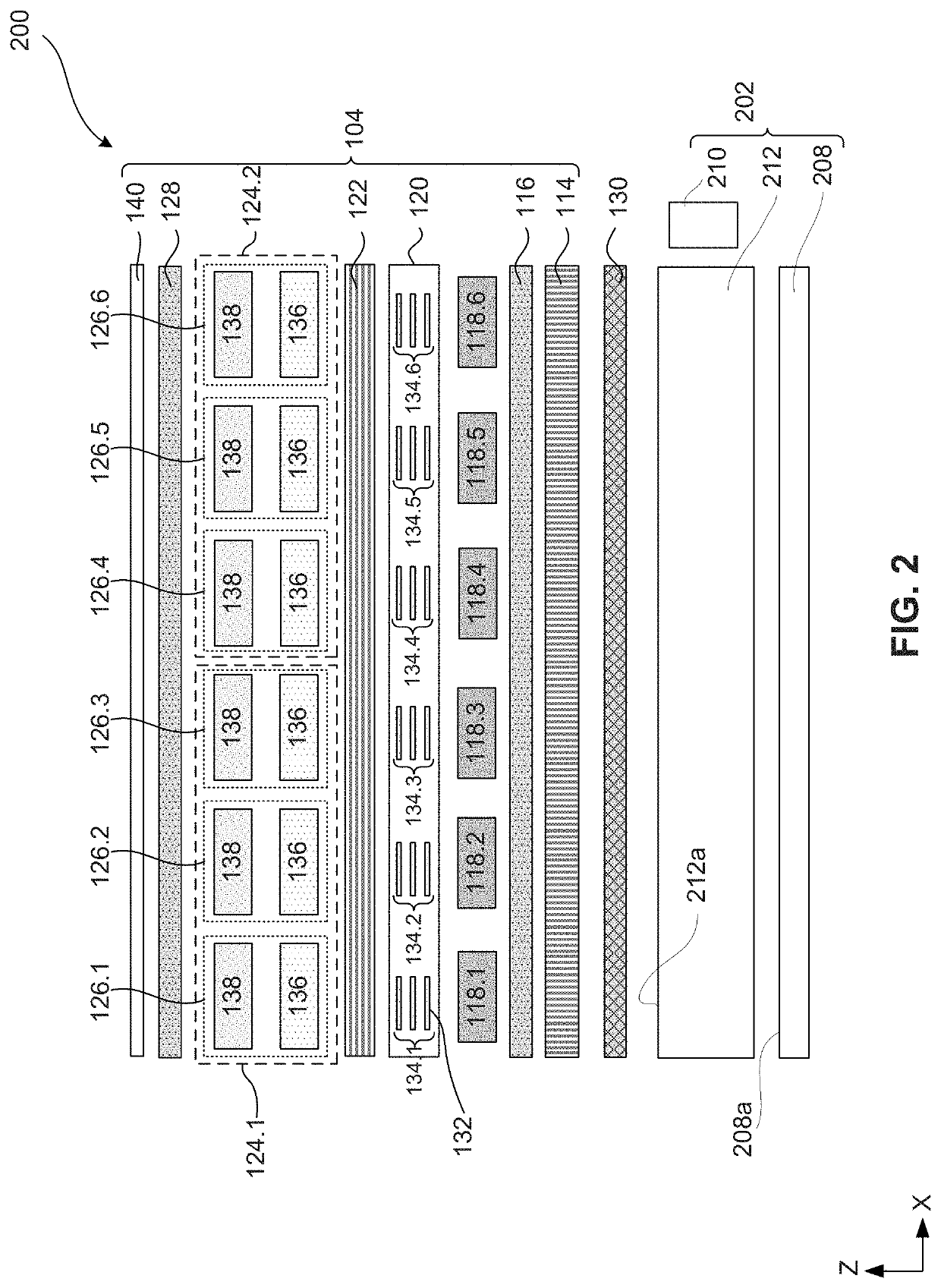
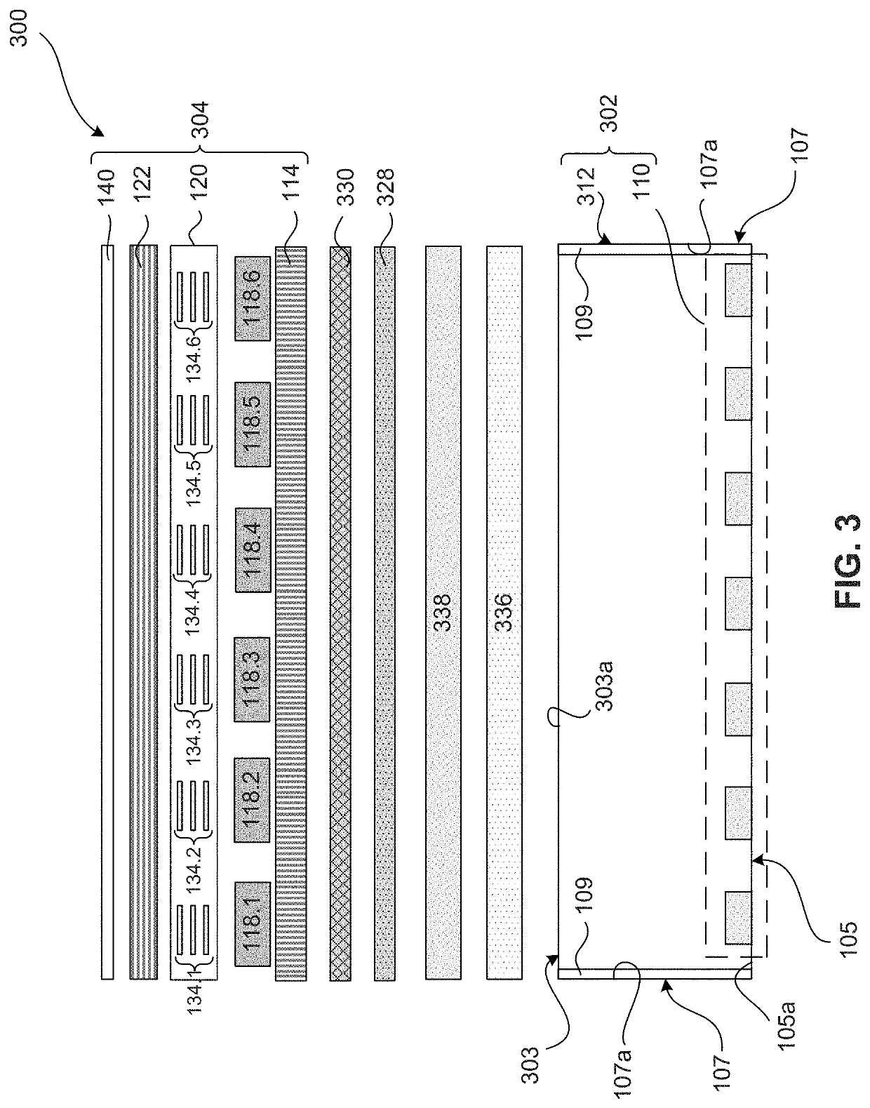
[0022]Although specific configurations and arrangements may be discussed, it should be understood that this is done for illustrative purposes only. A person skilled in the pertinent art will recognize that other configurations and arrangements can be used without departing from the spirit and scope of the present invention. It will be apparent to a person skilled in the pertinent art that this invention can also be employed in a variety of other applications beyond those specifically mentioned herein. It should be appreciated that the particular implementations shown and described herein are examples and are not intended to otherwise limit the scope of the application in any way.

[0023]It is noted that references in the specification to “one embodiment,”“an embodiment,”“an example embodiment,” etc., indicate that the embodiment described may include a particular feature, structure, or characteristic, but every embodiment may not necessarily include the particular feature, structure, ...


PUM

PropertyMeasurementUnit
diameteraaaaaaaaaa
sizesaaaaaaaaaa
sizesaaaaaaaaaa

Abstract

A display device is provided having a quantum dot formed directly on a surface or substrate of a backlight unit, without requiring an intervening layer. An optically transmissive layer is formed thereon. The quantum dot film may be provided that includes a population of optical features to permit the omission of additional films, such as a separate optical film. A population of optical features may include a population of embedded microspheres to achieve optical effects, to improve the overall thickness uniformity of the quantum dot film, or both. Additionally or alternatively, the quantum dot film may be provided having optical features embossed thereon, such as reflective and / or refractive features, prisms, grooves, grooved prisms, lenticular lenses, micro-lenses, micro-spheres, any other lenses, pitches, or other suitable brightness enhancement and / or optical features. Thereby, a separate optical film may be omitted from the overall device structure.

Description

CROSS REFERENCE TO RELATED APPLICATION[0001]The present application claims the benefit of U.S. Provisional Patent Appl. No. 62 / 702,776, filed Jul. 24, 2018, titled “Methods Of Improving Efficiency Of Displays Using Quantum Dots With Integrated Optical Elements,” which is incorporated herein by reference in its entirety.FIELD[0002]This disclosure is generally related to display devices and, more specifically, display devices including luminescent nanocrystals such as quantum dots (QDs).BACKGROUND[0003]Display devices (e.g., liquid crystal displays (LCDs)) are used as screens or displays for a wide variety of electronic devices and typically require some form of backlighting for images to be visible in normal or reduced ambient light environments. In a backlight unit (BLU) of the display device, LEDs are typically utilized as a light source. The LEDs may be arranged around the edge or perimeter of the display device. The BLU may also utilize phosphors, such as yttrium-aluminum-garnet ...

Claims


Application Information

Patent Timeline
Patent Type & Authority Applications(United States)
IPC IPC(8): F21V8/00G02F1/1335
CPCG02F1/133617G02F2001/133607G02F1/133603G02B6/0053G02F2001/133614G02F1/133606G02F1/133512G02F1/133602G02F1/133615G02F1/1333G02F1/133614G02B6/005G02B6/0043H01L31/035218G02F1/133607H10K50/121
Inventor LEE, ERNEST CHUNG-WEI
Owner SHOEI CHEM IND CO LTD
Why Eureka
Try Eureka