
Transparent planar heating film including transferred metal nanoparticles and method for manufacturing the same
a technology of transparent planar heating and metal nanoparticles, which is applied in the direction of ohmic resistance heating, ohmic resistance heating details, electrical equipment, etc., can solve the problems of difficult to activate the transparent planar heating film for a long time, local overheating inability to completely eliminate the occurrence of fogging or dew condensation. , to achieve the effect of improving the strength of the transparent planar heating film, low haz
- Summary
- Abstract
- Description
- Claims
- Application Information
AI Technical Summary
Benefits of technology
Problems solved by technology
Method used
Image

Examples
example 1
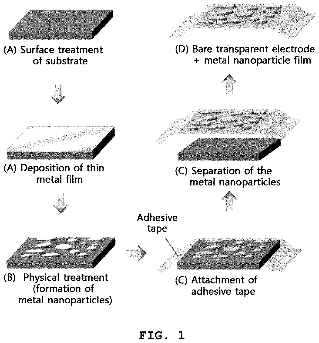
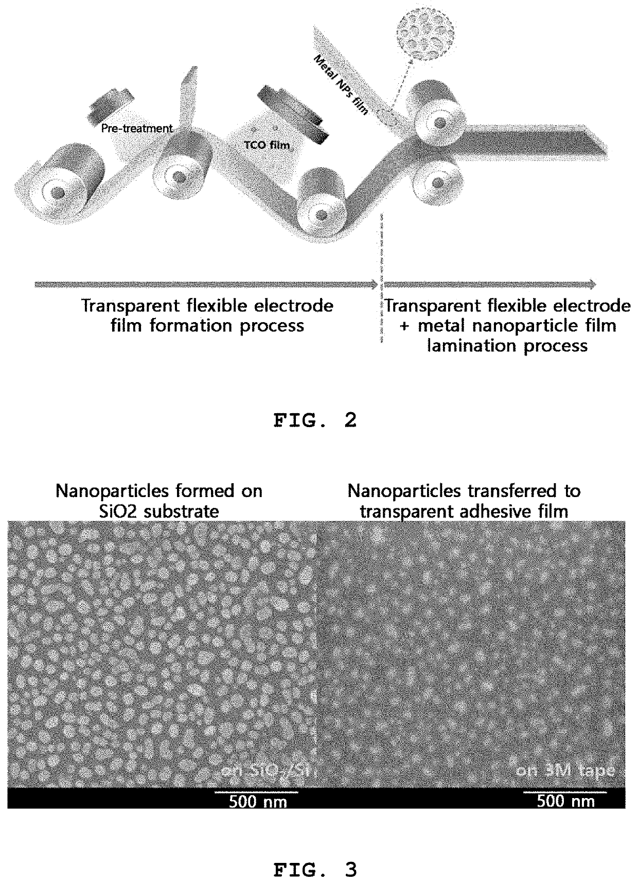
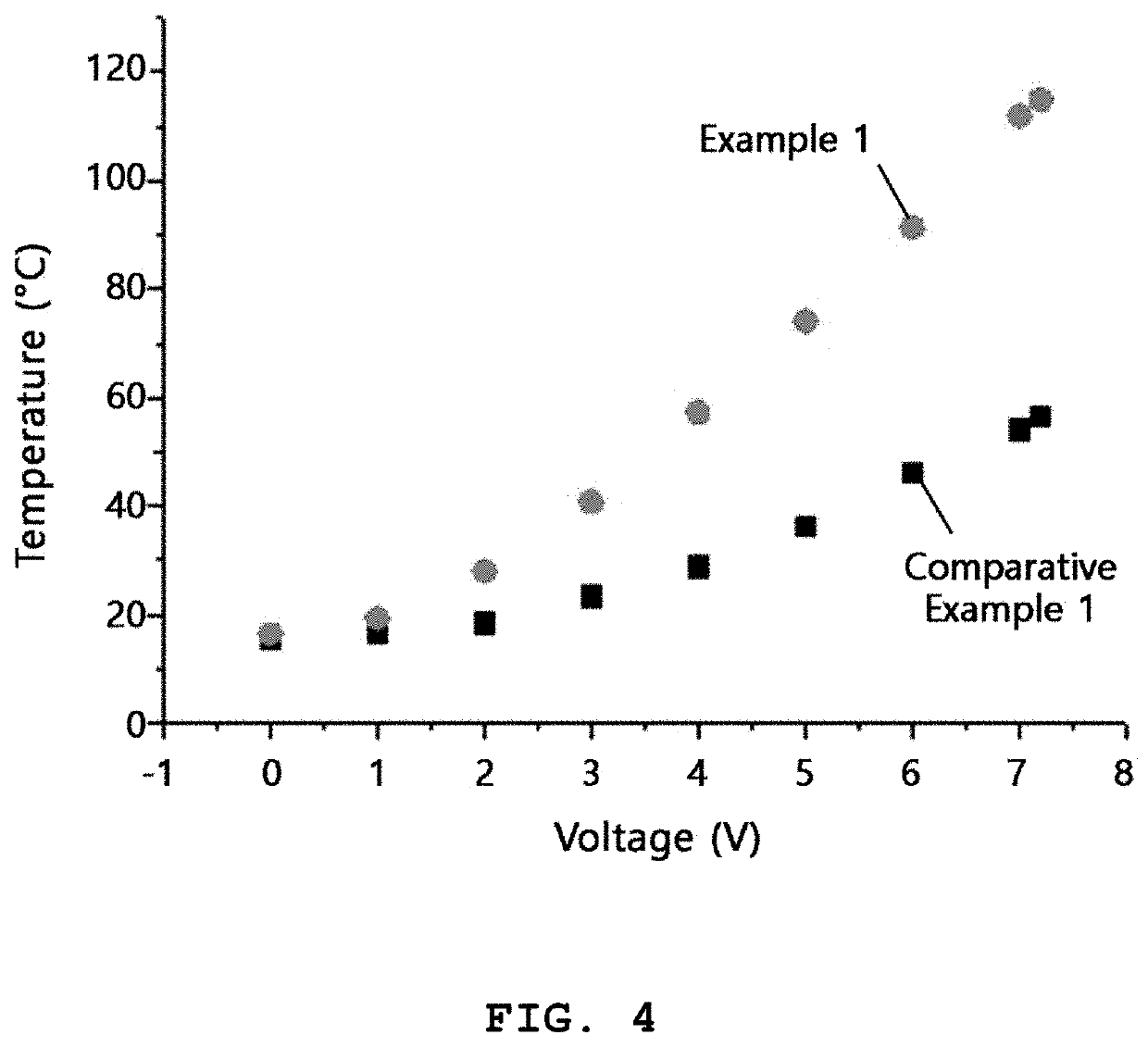
[0056]A SiO2 substrate was immersed in a DTS solution (a mixture of 1 ml of trichlorododecylsilane and 20 ml of toluene) at room temperature for 1 h, sonicated in toluene, and deposited with silver (Ag) to a thickness of 10 nm using a thermal evaporator. The deposited thin silver film was annealed in a furnace at 200° C. for 20 min to form metal nanoparticles with an average diameter of 130 nm. The metal nanoparticles formed on the SiO2 substrate are shown in the left SEM image of FIG. 3. An adhesive film was attached to the surface of the SiO2 substrate where the metal nanoparticles were formed, and was then detached from the substrate. At this time, the metal nanoparticles were naturally separated from the substrate. The resulting adhesive film attached with the metal nanoparticles (see the right SEM image of FIG. 3) was attached to a transparent electrode by using a roll-to-roll process, as illustrated in FIG. 2, such that the metal nanoparticles were brought into contact with th...
PUM
| Property | Measurement | Unit |
|---|---|---|
| diameter | aaaaa | aaaaa |
| transparent | aaaaa | aaaaa |
| diameter | aaaaa | aaaaa |
Abstract
Description
Claims
Application Information