Manufacturing method of chip package and chip package

a manufacturing method and chip technology, applied in the direction of electrical equipment, semiconductor devices, semiconductor/solid-state device details, etc., can solve the problems of difficult to improve product yield, and the foregoing chip package cannot be applied to different types of optical sensors, so as to improve reliability, less pollution, and easy separation

Active Publication Date: 2020-05-07
XINTEC INC
View PDF0 Cites 1 Cited by
  • Summary
  • Abstract
  • Description
  • Claims
  • Application Information

AI Technical Summary

Benefits of technology

[0062]Referring to FIG. 16, the package structure 200 is cut from the top surface 232 of the carrier 230 with a modified laser L. The modified laser L differs from a general laser in that the modified laser L does not use destructive processing, but uses a mechanism of stress release in a workpiece to cause a crack, so the modified laser L has less pollution and improves reliability compared with conventional cutting. The modified laser lens L focuses on the inside of an object to be cut, and scans in a horizontal direction to make the object to be cut generate an internal crack, which makes it easy to achieve separation by stress in a subsequent process. Since the modified laser L can be used to cut a composite material, in addition to cutting the carrier 230, the modified laser L can further cut the supporting part 240 and the wafer 210 below the carrier 230. The modified laser L is used for the purpose of cutting in a sintering manner and focuses on a depth range of the object to be cut to form a crack inside the object to be cut.
[0063]As shown in FIG. 23, after the carrier 230 is cut with the modified laser L, an internal stress layer 203 can be formed in an interior of the carrier 230 (namely a side face 234 after the cutting) and a crack 204 can be formed extending up and down from the internal stress layer 203. Adjustment parameters of the modified laser L can be determined according to a laser wavelength and a type and a thickness of the object to be cut. The modified laser L can save the process steps of cutting the wafer level package and reduce the volume of a material removed to avoid waste. In addition, the advantages of the modified laser L further include less heat affect zone (HAZ), less chipping, smaller debris (Debris), less contamination, higher cutting speed, and less scribe line area. The size of the debris can be less than 10 μm.

Problems solved by technology

However, when the function layer and the carrier are being cut, the sensing area is susceptible to damage, such as contamination, which makes it difficult to improve the product yield.
As a result, the foregoing chip package cannot be applied to different types of optical sensors.

Method used


Image

  • Manufacturing method of chip package and chip package
  • Manufacturing method of chip package and chip package
  • Manufacturing method of chip package and chip package

Examples


Embodiment Construction

[0042]Reference will now be made in detail to the present embodiments of the invention, examples of which are illustrated in the accompanying drawings. Wherever possible, the same reference numbers are used in the drawings and the description to refer to the same or like parts.

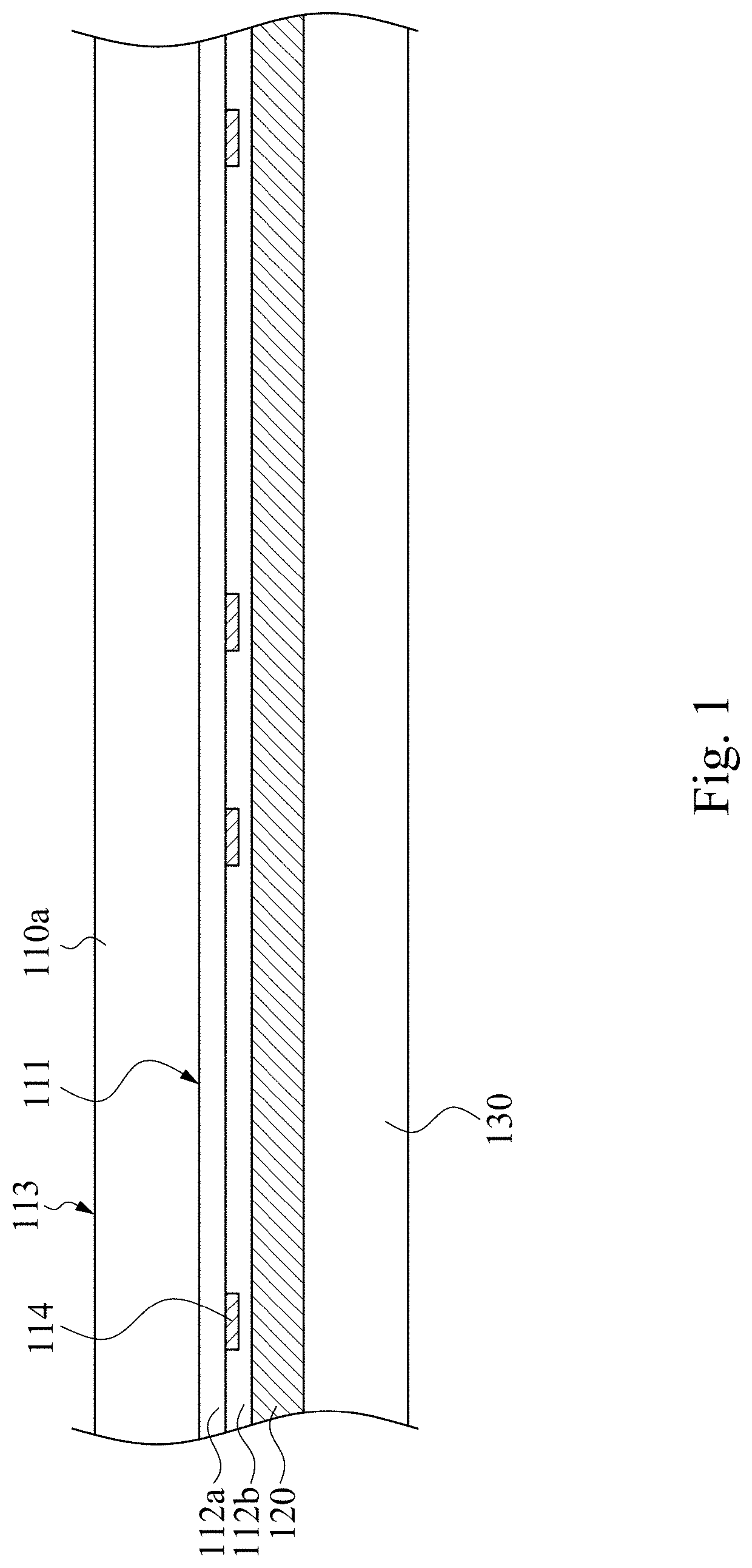
[0043]FIGS. 1-11 illustrate cross-sectional views of steps of a manufacturing method of a chip package according to an embodiment of the present invention. Referring to FIG. 1, a wafer 110a and a light-transmissive function layer 120 are bonded to a carrier 130, such that the light-transmissive function layer 120 is located between the wafer 110a and the carrier 130. After the wafer 110a and the light-transmissive function layer 120 are bonded to the carrier 130, a surface 113 of the wafer 110a facing away from the light-transmissive function layer 120 can be ground. In this embodiment, the wafer 110a has a first isolation layer 112a and a second isolation layer 112b on the light-transmissive function layer 12...


PUM

PropertyMeasurementUnit
sizeaaaaaaaaaa
included angleaaaaaaaaaa
conductiveaaaaaaaaaa

Abstract

A manufacturing method of a chip package includes patterning a wafer to form a scribe trench, in which a light-transmissive function layer below the wafer is in the scribe trench, the light-transmissive function layer is between the wafer and a carrier, and a first included angle is formed between an outer wall surface and a surface of the wafer facing the light-transmissive function layer; cutting the light-transmissive function layer and the carrier along the scribe trench to form a chip package that includes a chip, the light-transmissive function layer, and the carrier; and patterning the chip to form an opening, in which the light-transmissive function layer is in the opening, a second included angle is formed between an inner wall surface of the chip and a surface of the chip facing the light-transmissive function layer, and is different from the first included angle.

Description

RELATED APPLICATIONS[0001]This application claims priority to U.S. Provisional Application Ser. No. 62 / 754,349, filed Nov. 1, 2018, and U.S. Provisional Application Ser. No. 62 / 900,949, filed Sep. 16, 2019, which are herein incorporated by reference.BACKGROUNDField of Invention[0002]The present invention relates to a manufacturing method of a chip package and a chip package.Description of Related Art[0003]Generally, when a chip package for sensing light is being manufactured, a wafer and a function layer can be first bonded to a carrier, and then the wafer is subjected to an etching process such that an opening of a sensing area and a scribe trench for a subsequent cutting process can be simultaneously formed on the wafer. In a subsequent process, an isolation layer of the wafer in the opening can be removed to expose the function layer, and then a step of cutting the function layer and the carrier along the scribe trench is performed to form a chip package.[0004]However, when the f...

Claims


Application Information

Patent Timeline
Patent Type & Authority Applications(United States)
IPC IPC(8): H01L21/768H01L21/02H01L23/00
CPCH01L21/02013H01L21/76894H01L24/94H01L21/3043H01L31/1804H01L31/02161H01L31/02363H01L31/02327H01L21/78H01L23/481H01L2224/94H01L2224/32225H01L2224/13022H01L2224/13024H01L2224/02379H01L2224/02372H01L2224/05548H01L24/05H01L24/03H01L2224/0556H01L2224/83H01L2224/11H01L2224/03H01L2924/00012
Inventor LIN, CHIA-SHENGWU, HUI-HSIENCHEN, JIAN-HONGLIU, TSANG-YUCHEN, KUEI-WEI
Owner XINTEC INC
Why Eureka
Try Eureka