Wafer support

a technology of a wafer and a support plate, which is applied in the direction of ceramic layered products, layered products, chemistry apparatus and processes, etc., can solve the problem of non-uniform density of plasma

Active Publication Date: 2020-05-21
NGK INSULATORS LTD
View PDF3 Cites 4 Cited by
  • Summary
  • Abstract
  • Description
  • Claims
  • Application Information

AI Technical Summary

Benefits of technology

[0017]In the wafer support according the present invention, the plurality of RF zone electrodes may include a circular electrode concentric to the ceramic base and one or more annular electrodes concentric to the ceramic base, the annular electrodes being positioned outside the circular electrode, the plurality of heater zone electrodes constituting the heater electrode may be disposed on the same plane, and heights of the plurality of RF zone electrodes from the heater electrode may be set such that the height of the RF zone electrode positioned closer to a center of the ceramic base is higher (or lower). In such a case, thicknesses of the ceramic base in regions above the RF zone electrodes (namely, thicknesses of dielectric layers in those regions) may be equal to each other.

Problems solved by technology

Therefore, density of the plasma becomes non-uniform in some cases.

Method used


Image

  • Wafer support
  • Wafer support
  • Wafer support

Examples


Embodiment Construction

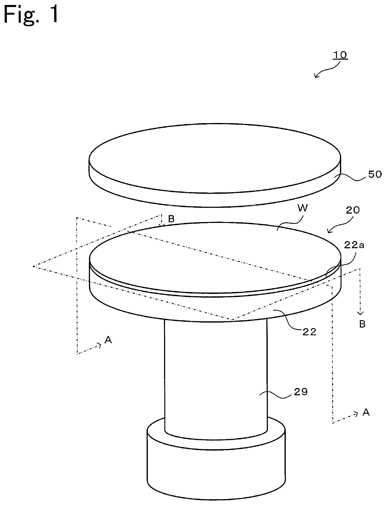
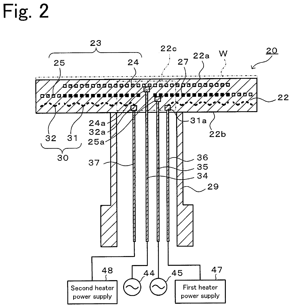
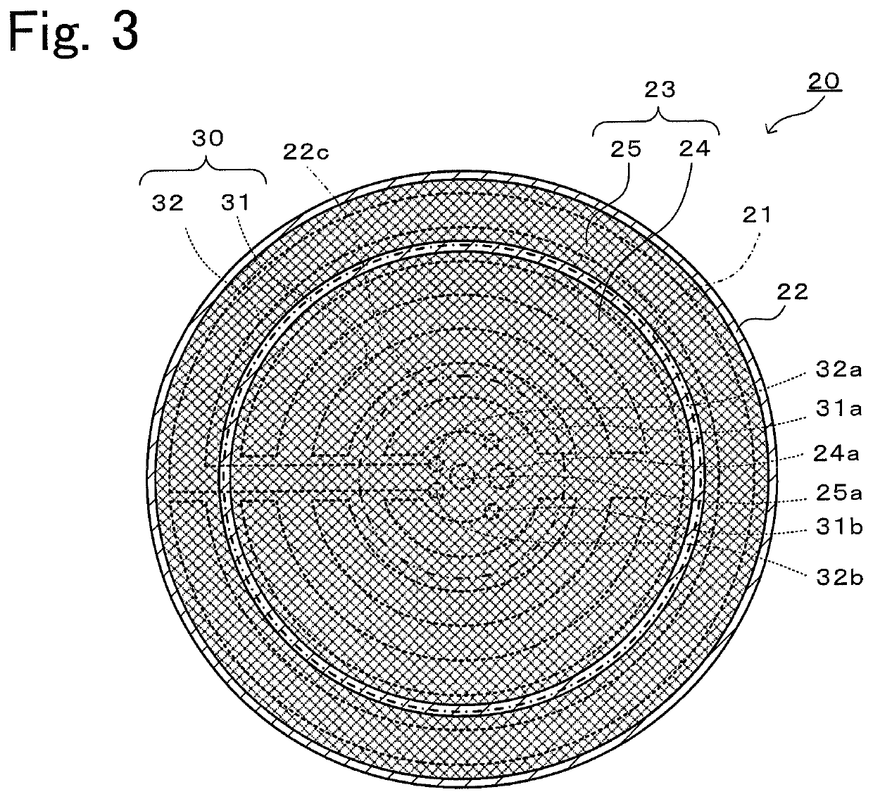
[0032]A preferred embodiment of the present invention will be described below with reference to the drawings. FIG. 1 is a perspective view of the plasma generator 10. FIG. 2 is a sectional view taken along A-A in FIG. 1, and FIG. 3 is a sectional view taken along B-B in FIG. 1. FIG. 4 is a perspective view illustrating an arrangement of an RF electrode 23 and a heater electrode 30.

[0033]As illustrated in FIG. 1, the plasma generator 10 includes a wafer support 20 and an upper electrode 50.

[0034]The wafer support 20 is used to support and heat a wafer W on which CVD, etching, etc. are performed with the aid of plasma, and it is mounted inside a not-illustrated chamber for a semiconductor process. The wafer support 20 includes a ceramic base 22 and a hollow ceramic shaft 29.

[0035]As illustrated in FIG. 2, the ceramic base 22 is a disk-shaped member made of ceramic (alumina or aluminum nitride). A front surface of the ceramic base 22 serves as a wafer placement surface 22a on which the...


PUM

PropertyMeasurementUnit
temperatureaaaaaaaaaa
distancesaaaaaaaaaa

Abstract

A wafer support includes an RF electrode and a heater electrode that are embedded inside a disk-shaped ceramic base having a wafer placement surface. The RF electrode is constituted by a plurality of RF zone electrodes that are individually disposed for each of a plurality of divided zones of the wafer placement surface. The plurality of RF zone electrodes are separately disposed in at least two stages that are positioned at different distances from the wafer placement surface. The heater electrode is constituted by a plurality of heater zone electrodes that are individually disposed for each of a plurality of divided zones of the wafer placement surface, the zones being divided in a similar or different way to or from the RF zone electrodes.

Description

BACKGROUND OF THE INVENTION1. Field of the Invention[0001]The present invention relates to a wafer support.2. Description of the Related Art[0002]In a known wafer support, an RF electrode and a heater electrode are embedded inside a disk-shaped ceramic base having a wafer placement surface in the mentioned order from the side closer to the wafer placement surface. The above-type wafer support disclosed in Patent Literature (PTL) 1, for example, includes a circular RF electrode and an annular RF electrode that are embedded inside the ceramic base at different depths from the wafer placement surface. A flat-plate upper electrode is disposed at a position opposing to the wafer placement surface of the wafer support. Plasma is generated by applying radio frequency power between a parallel-plate electrode constituted by the flat-plate upper electrode and each of the RF electrodes in the wafer support. PTL 1 states that a density distribution of plasma can be satisfactorily controlled by ...

Claims


Application Information

Patent Timeline
Patent Type & Authority Applications(United States)
IPC IPC(8): H01J37/32H01L21/67B32B18/00H01L21/687
CPCH01J37/32724H01J37/32577H01L21/68757H01L21/68785B32B18/00H01J37/32541H01J37/32568H01L21/67248H01L21/68735H01L21/68792H01L21/67103C04B37/006C04B37/001C04B2237/343C04B2237/366C04B2237/765C04B2237/80H01L21/205
Inventor TAKAHASHI, TOMOHIRO
Owner NGK INSULATORS LTD
Why Eureka
Try Eureka