Touch screen and display device

a display device and touch screen technology, applied in the field of touch control technology, can solve the problems of increasing the difficulty of bonding, increasing the number of bonded terminals, and large circuit size, and achieve the effects of reducing the number of terminals in the bonding area, reducing the number of channels required for the single-layer matrix self-capacitive touch screen, and reducing the size of the integrated circui

Inactive Publication Date: 2020-06-04
WUHAN CHINA STAR OPTOELECTRONICS SEMICON DISPLAY TECH CO LTD
View PDF3 Cites 1 Cited by
  • Summary
  • Abstract
  • Description
  • Claims
  • Application Information

AI Technical Summary

Benefits of technology

[0038]The benefits of the present application are: compared with the touch screen of the prior art, the touch screen and the display device provided by the present application are added with switch signals and utilize the control of the thin film transistors, and one channel can transmit and receive signals in time division for multiple touch control electrodes. Therefore, the number of channels required for the single-layer matrix self-capacitive touch screen is reduced, thereby reducing the integrated circuit size, reducing the number of terminals in the bonding area, and greatly reducing the difficulty of bonding.

Problems solved by technology

Because the number of channels of the matrix touch control electrodes is too large, to achieve the same precision as the mutual capacitive touch screen, a number of channels far more than that of the mutual capacitive touch screen is required; generally, the number of channels required for the matrix self-capacitive touch screen is large, which makes the integrated circuit size larger, and also causes a larger number of bonded terminals, thereby increasing the difficulty of bonding.
Therefore, the prior art possesses drawbacks and is in urgent need of improvement.

Method used


Image

  • Touch screen and display device

Examples


Embodiment Construction

[0042]The following descriptions for the respective embodiments are specific embodiments capable of being implemented for illustrations of the present invention with referring to appended figures. The terms of up, down, front, rear, left, right, interior, exterior, side, etcetera are merely directions of referring to appended figures. Thus, the used directional terms are used to describe and understand the present invention, but the present invention is not limited thereto. In the figure, units with similar structures are denoted by the same reference numerals.

[0043]The present application is directed to the touch screen of the prior art, in which the number of channels required for the single-layer matrix self-capacitive touch screen is more, which leads to the technical problem of increasing the IC size, to increasing the number of terminals in the bonding area, and the difficulty in bonding. This embodiment can solve these drawbacks.

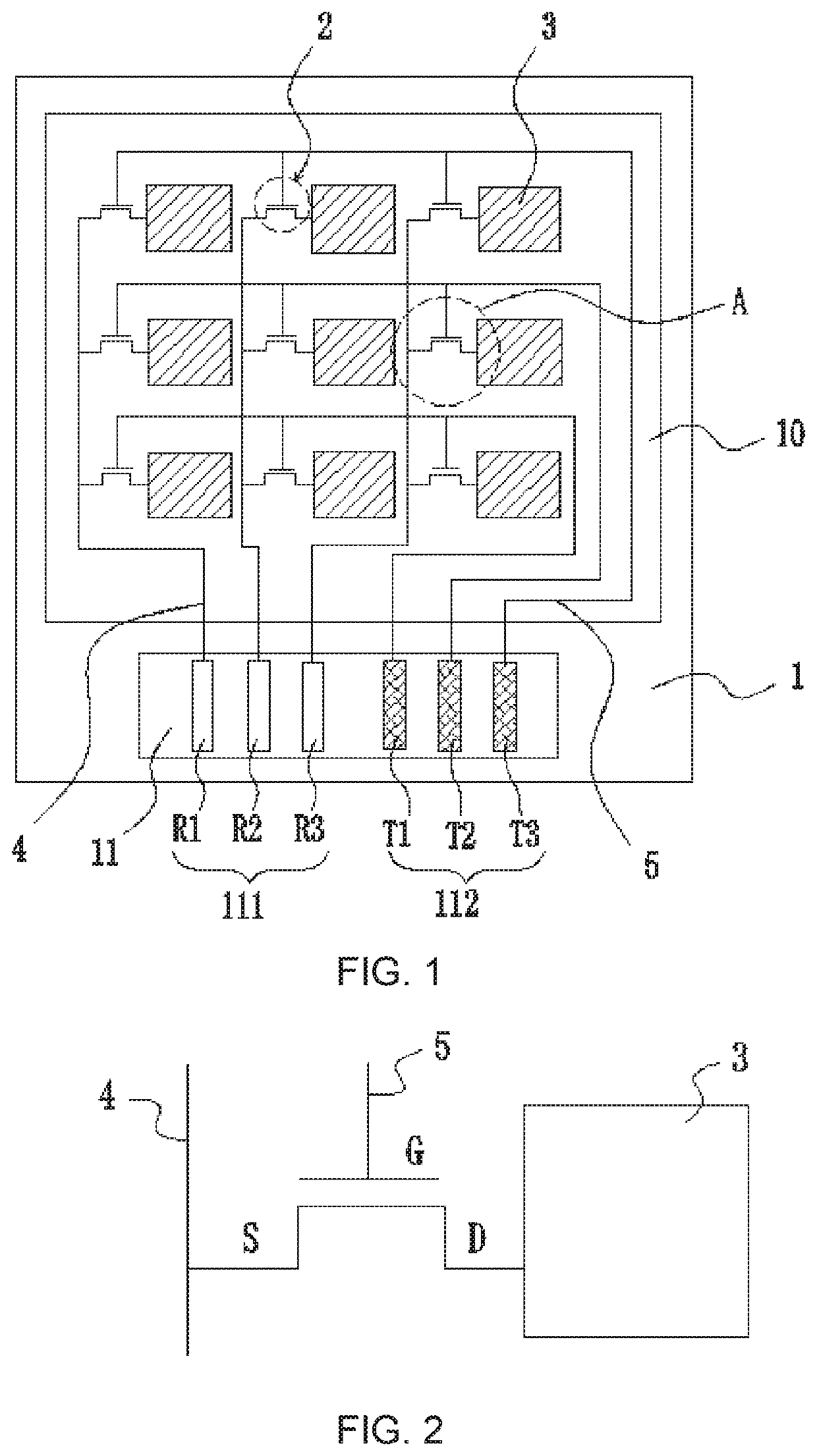
[0044]Please refer to FIG. 1, which is a struct...


PUM

PropertyMeasurementUnit
areaaaaaaaaaaa
sizeaaaaaaaaaa
structuresaaaaaaaaaa

Abstract

Provided are a touch screen and a display device. The touch screen includes: thin film transistors and touch control electrodes disposed on the substrate, and the substrate includes signal channels for transmitting or receiving the touch control electrode capacitive signal in time division and control channels for controlling on and off of the thin film transistors; sources of at least two of the thin film transistors connect one signal trace to one signal channel; gates of the at least two of the thin film transistors connect one control trace to one control channel; one touch control electrode is connected to a drain of one thin film transistor.

Description

FIELD OF THE INVENTION[0001]The present application relates to a touch control technology field, and more particularly to a touch screen and a display device.BACKGROUND OF THE INVENTION[0002]At present, if a self-capacitive touch screen needs to implement multi-touch (such as five-points touch control), single-layer matrix touch control electrodes are needed. Each touch control electrode needs a corresponding signal channel, and when a finger touches, the signal amount of the touch control electrode in the finger area is changed, thereby determining the touch position; since each touch control electrode is independent, it can support multi-touch because the interference with each other will not occur.[0003]Because the number of channels of the matrix touch control electrodes is too large, to achieve the same precision as the mutual capacitive touch screen, a number of channels far more than that of the mutual capacitive touch screen is required; generally, the number of channels req...

Claims


Application Information

Patent Timeline
Patent Type & Authority Applications(United States)
IPC IPC(8): G06F3/041G06F3/044
CPCG06F3/0446G06F3/04166G06F3/0443G06F3/04164
Inventor MA, YALONG
Owner WUHAN CHINA STAR OPTOELECTRONICS SEMICON DISPLAY TECH CO LTD
Why Eureka
Try Eureka