
Organic Light Emitting Display Apparatus

a light-emitting display and organic technology, applied in electrical devices, semiconductor devices, organic semiconductor devices, etc., can solve problems such as abnormal driving, dark spots, and bright spot defects, and achieve the effects of reducing reliability, simplifying structure, and minimizing or reducing problems

Active Publication Date: 2020-07-02
LG DISPLAY CO LTD
View PDF0 Cites 5 Cited by
  • Summary
  • Abstract
  • Description
  • Claims
  • Application Information

AI Technical Summary

Benefits of technology

The present invention provides an organic light emitting display apparatus with a simplified structure that allows for repair treatment of sub pixels with bright spots. The repair treatment can help improve the yield of the display and minimize damage to the sub pixel. The invention also includes a transparent organic light emitting display apparatus with a sub pixel structure that facilitates a repair treatment. Overall, the technical effects of the invention include improved repair treatment efficiency and reduced likelihood of damage or lowered reliability of the sub pixel.

Problems solved by technology

However, the organic light emitting device having the above structure may have defects of abnormal driving caused by a deterioration of the thin film transistor properties and an internal short of the thin film transistor for a process of manufacturing lines and switching and driving thin film transistors.
If the thin film transistor formed in one pixel area is not driven normally, a current or voltage is not applied to the organic light emitting device connected with the thin film transistor, whereby it may cause dark spots therein.
Thus, the pixel area to be driven is in a turning-on state, to thereby cause defects of bright spots.
Especially, the bright spots may be clearly visible to a user, to thereby deteriorate a picture quality.
Thus, even though only one spot occurs in a front surface of a display area, it becomes a defective display device, whereby it cannot be used for a final product.

Method used


Image

  • Organic Light Emitting Display Apparatus
  • Organic Light Emitting Display Apparatus
  • Organic Light Emitting Display Apparatus

Examples


Embodiment Construction

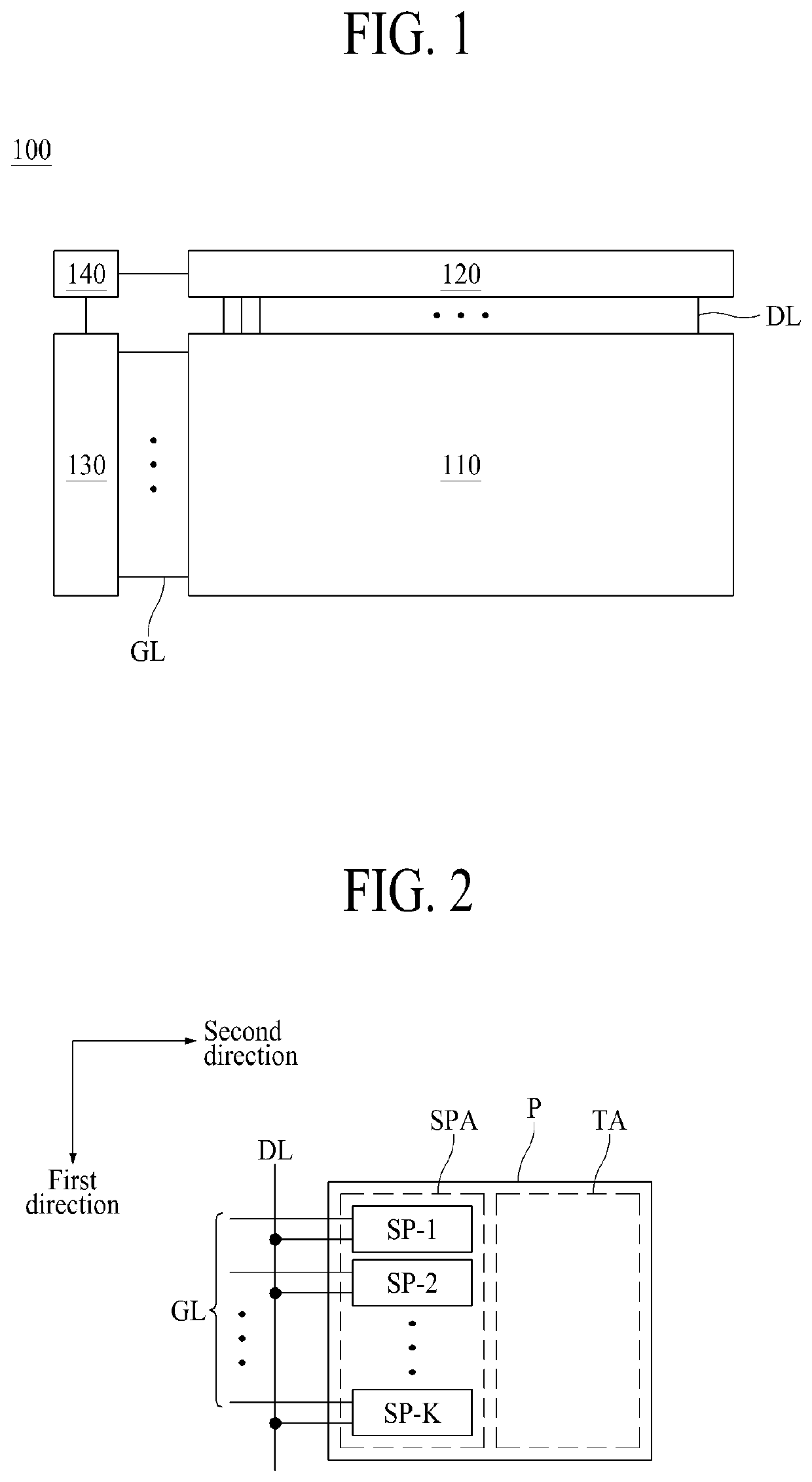
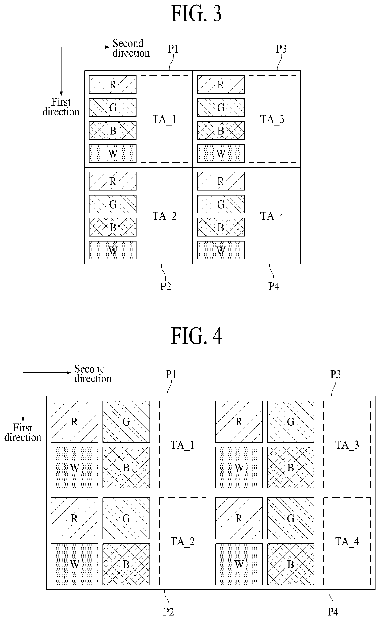
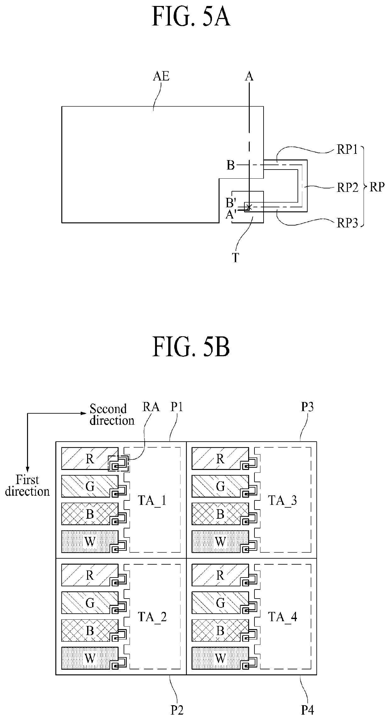
[0032]Advantages and features of the present disclosure, and implementation methods thereof will be clarified through following embodiments described with reference to the accompanying drawings. The present disclosure may, however, be embodied in different forms and should not be construed as limited to the embodiments set forth herein. Rather, these embodiments are provided so that this disclosure will be thorough and complete, and will fully convey the scope of the present disclosure to those skilled in the art. Further, the present disclosure is only defined by scopes of claims.

[0033]A shape, a size, a ratio, an angle, and a number disclosed in the drawings for describing embodiments of the present disclosure are merely an example, and thus, the present disclosure is not limited to the illustrated details. Like reference numerals refer to like elements throughout the specification. In the following description, when the detailed description of the relevant known function or confi...


PUM

PropertyMeasurementUnit
thicknessaaaaaaaaaa
areaaaaaaaaaaa
insulatingaaaaaaaaaa

Abstract

An organic light emitting display apparatus is disclosed, wherein the organic light emitting display apparatus comprises a driving thin film transistor provided on a substrate and disposed in a pixel area including a plurality of sub pixels; an organic light emitting diode electrically connected with the driving thin film transistor; and a repair portion provided at one side of the organic light emitting diode, wherein the organic light emitting diode is electrically connected with the driving thin film transistor through the repair portion.

Description

CROSS-REFERENCE TO RELATED APPLICATION[0001]This application claims the benefit of Republic of Korea Patent Application No. 10-2018-0170851, filed on Dec. 27, 2018, which is hereby incorporated by reference in its entirety.BACKGROUNDTechnical Field[0002]The present disclosure relates to an organic light emitting display apparatus.Discussion of the Related Art[0003]With the advancement of an information-oriented society, a display apparatus for displaying information has been developed in various types. Recently, various display apparatuses such as a liquid crystal display (LCD) apparatus, a plasma display apparatus, and an organic light emitting display (OLED) apparatus have been utilized.[0004]The organic light emitting display apparatus largely includes an array device and an organic light emitting device. The array device includes a switching thin film transistor connected with gate and data lines, and at least one driving thin film transistor connected with the organic light emi...

Claims


Application Information

Patent Timeline
Patent Type & Authority Applications(United States)
IPC IPC(8): H01L27/32H01L51/56
CPCH01L51/56H01L27/3272H01L27/3258H01L27/3223H01L27/3262H01L2251/568H01L27/3279H10K59/122H10K71/861H10K59/80H10K59/1315H10K59/351H10K59/88H10K59/35H10K59/123H10K59/124H10K59/126H10K59/1213H10K71/00
Inventor KIM, DOHYUNGLEE, SAEMLEENURIYOO, SEUNGWONLEE, JOONSUKPARK, SEONGWOO
Owner LG DISPLAY CO LTD
Learn More