
Multi-Dimensional Model Of Optical Dispersion

a multi-dimensional model and optical dispersion technology, applied in the field of optical characterization systems, can solve the problems of measurement technology suffering from any of a number of limitations, measurement technology is slow, measurement requires the destruction of samples, etc., and achieves the effect of robustness and high throughput tracking

Active Publication Date: 2020-09-17
KLA TENCOR TECH CORP
View PDF0 Cites 3 Cited by
  • Summary
  • Abstract
  • Description
  • Claims
  • Application Information

AI Technical Summary

Benefits of technology

The patent presents methods and systems for estimating parameters of interest in a sample using optical measurements. It introduces a model called multidimensional optical dispersion (MDOD) that can track multiple parameters, such as fabrication control parameters, structural parameters, material composition parameters, and electrical parameters, among others. The MDOD model is based on physics and is flexible and robust in measuring various dispersion models. The technical effects of this invention are the early and accurate estimation of parameters of interest in a sample, which can help in improving the quality and efficiency of production processes.

Problems solved by technology

Increasingly complex FINFET structures and gate all around structures are under development for current and future fabrication nodes.
Currently, however, these measurement technologies suffer from any of a number of limitations.
In some cases, the measurements require destruction of the sample.
In some cases, the measurement technology is slow, and must be separated from the production line.
Although, optical metrology tools are successfully employed to characterize the electrical characteristics of device materials and structures, in many examples, it has proven difficult to translate the measured electrical properties into fabrication process control inputs to improve yield.
Existing parameterized models suffer from an inability to track parameters that can be directly controlled during the manufacturing process (e.g., film thickness, process temperature, material concentration, etc.).
However, the use of multiple reference dispersions increases measurement complexity and computational effort.
This limitation renders the approach unsuitable for many current and future use cases.

Method used


Image

  • Multi-Dimensional Model Of Optical Dispersion
  • Multi-Dimensional Model Of Optical Dispersion
  • Multi-Dimensional Model Of Optical Dispersion

Examples


Embodiment Construction

[0036]Reference will now be made in detail to background examples and some embodiments of the invention, examples of which are illustrated in the accompanying drawings.

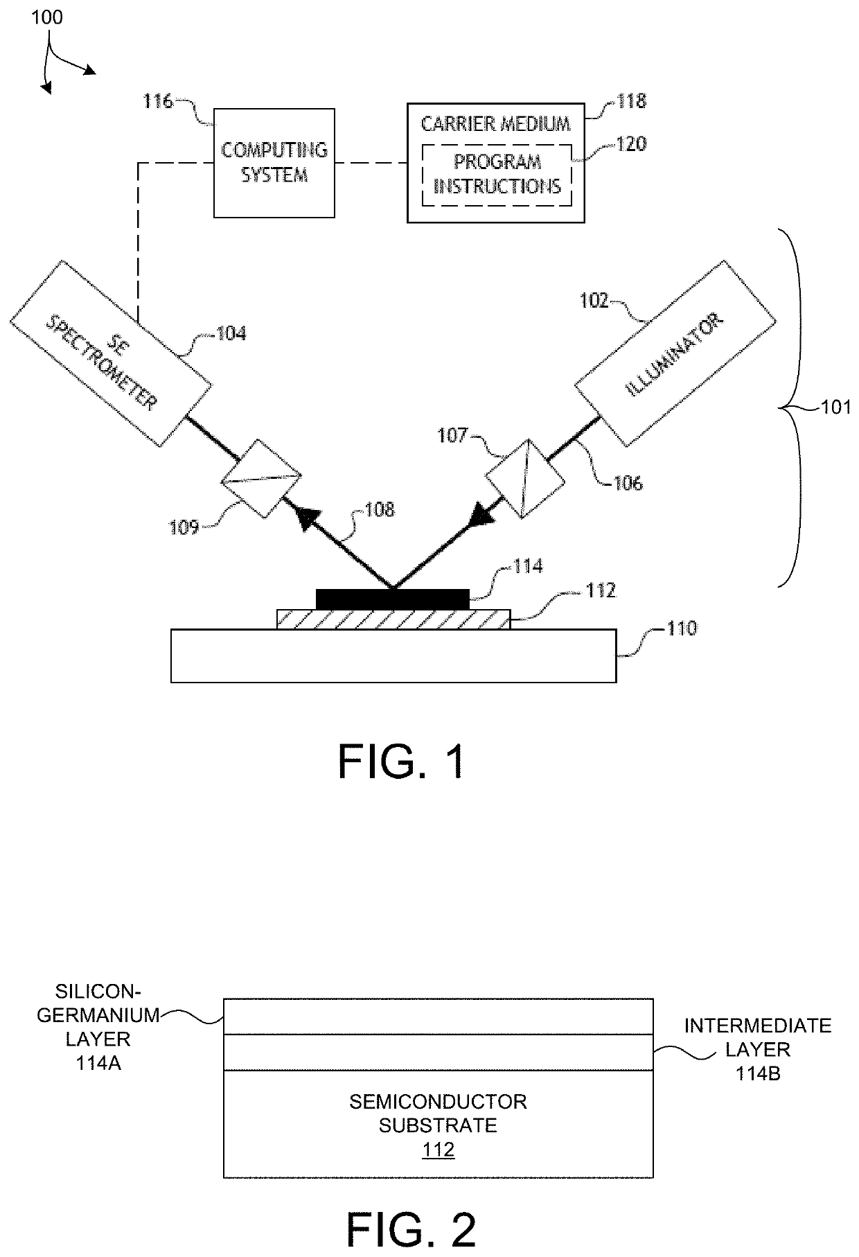
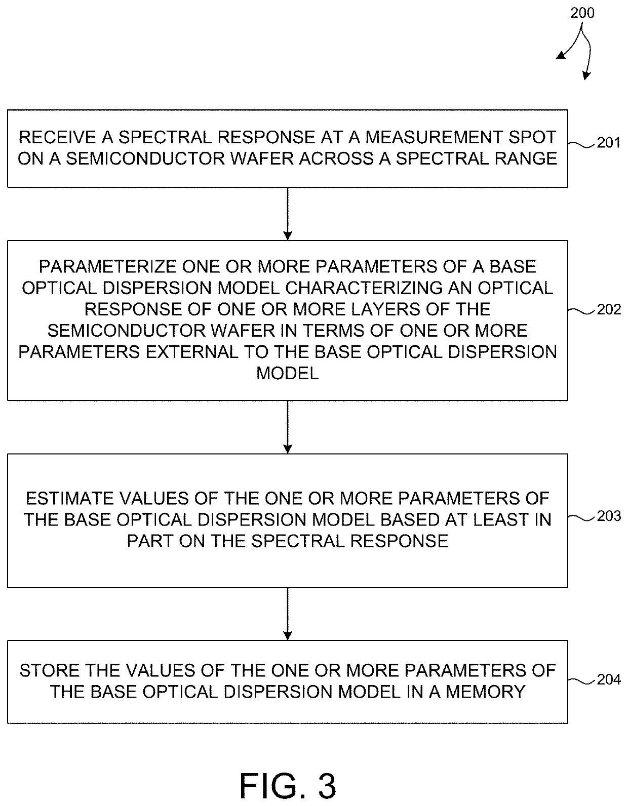
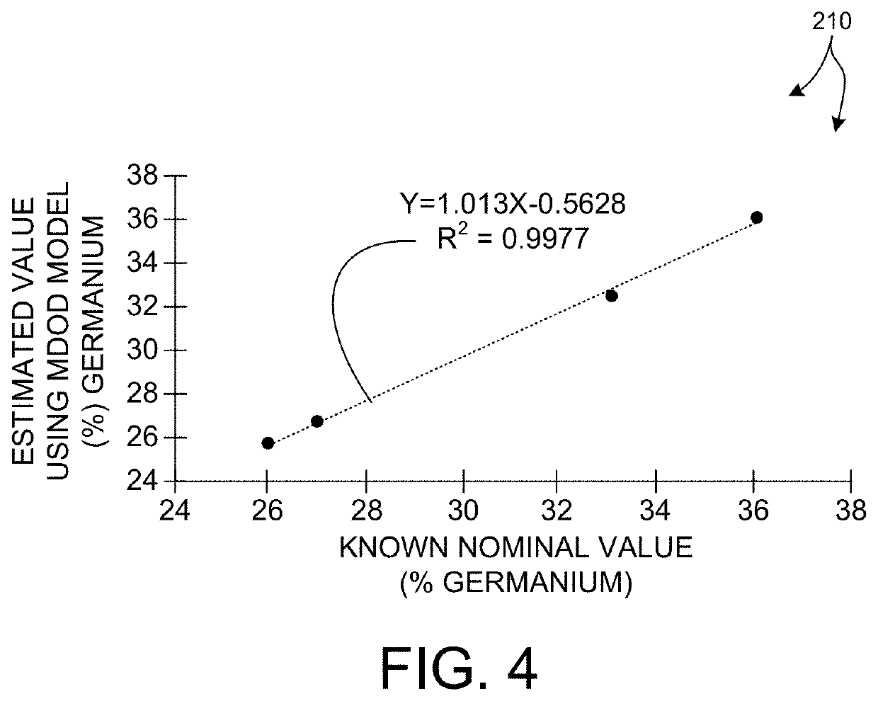
[0037]Methods and systems for estimating values of parameters of interest from optical measurements of a sample early in a production flow based on a multidimensional optical dispersion (MDOD) model are presented herein. The MDOD model enables robust, high throughput tracking of multiple parameters of interest, including fabrication control parameters, structural parameters, material composition parameters, electrical parameters, etc. In some measurement applications, measurement accuracy is improved and the computational effort required to develop the MDOD model is less than alternative techniques.

[0038]Current and future semiconductor structures include, but are not limited to, materials having optical dispersion properties that strongly depend on the particular device application of the materials and the processes ...


PUM


Abstract

Methods and systems for estimating values of parameters of interest from optical measurements of a sample early in a production flow based on a multidimensional optical dispersion (MDOD) model are presented herein. An MDOD model describes optical dispersion of materials comprising a structure under measurement in terms of parameters external to a base optical dispersion model. In some examples, a power law model describes the physical relationship between the external parameters and a parameter of the base optical dispersion model. In some embodiments, one or more external parameters are treated as unknown values that are resolved based on spectral measurement data. In some embodiments, one or more external parameters are treated as known values, and values of base optical dispersion model parameters, one or more external parameters having unknown values, or both, are resolved based on spectral measurement data and the known values of the one or more external parameters.

Description

CROSS REFERENCE TO RELATED APPLICATION[0001]The present application for patent claims priority under 35 U.S.C. § 119 from U.S. provisional patent application Ser. No. 62 / 819,658, entitled “Multidimensional Dispersion Model,” filed Mar. 17, 2019, the subject matter of which is incorporated herein by reference.TECHNICAL FIELD[0002]The described embodiments relate to systems for optical characterization of structures and materials employed in semiconductor manufacturing.BACKGROUND INFORMATION[0003]Semiconductor devices such as logic and memory devices are typically fabricated by a sequence of processing steps applied to a substrate or wafer. The various features and multiple structural levels of the semiconductor devices are formed by these processing steps. For example, lithography among others is one semiconductor fabrication process that involves generating a pattern on a semiconductor wafer. Additional examples of semiconductor fabrication processes include, but are not limited to,...

Claims


Application Information

Patent Timeline
IPC IPC(8): G01N21/95G01N21/956G01B11/06G06T7/00
CPCG01B11/0641G06T2207/30148G01N21/956G06T7/0004G01B2210/56G01N21/9501G01B11/0625G01N21/211G01N21/8422G01N21/41G01N21/9505H01L22/12H01L22/20G01R31/308G01R31/44G01N2201/12
Inventor MALKOVA, NATALIASUSHCHIK, MIKHAILHU, DAWEIYGARTUA, CARLOS L.
Owner KLA TENCOR TECH CORP
Learn More