Thin film circuit substrate and manufacturing method thereof

Active Publication Date: 2020-09-24
AMOGREENTECH CO LTD
View PDF2 Cites 0 Cited by
  • Summary
  • Abstract
  • Description
  • Claims
  • Application Information

AI Technical Summary

Benefits of technology

[0009]According to the present disclosure, the thin film circuit substrate and the manufacturing method thereof may form the photoresist layer through the electrospinning, thereby forming the thickness of the photoresist layer in a range of 1 μm to 5 μm.
[0010]In addition, the thin film circuit substrate

Problems solved by technology

However, with the lighter, thinner, shorter, and smaller trend of the

Method used


Image

  • Thin film circuit substrate and manufacturing method thereof
  • Thin film circuit substrate and manufacturing method thereof
  • Thin film circuit substrate and manufacturing method thereof

Examples


Example

BEST MODE

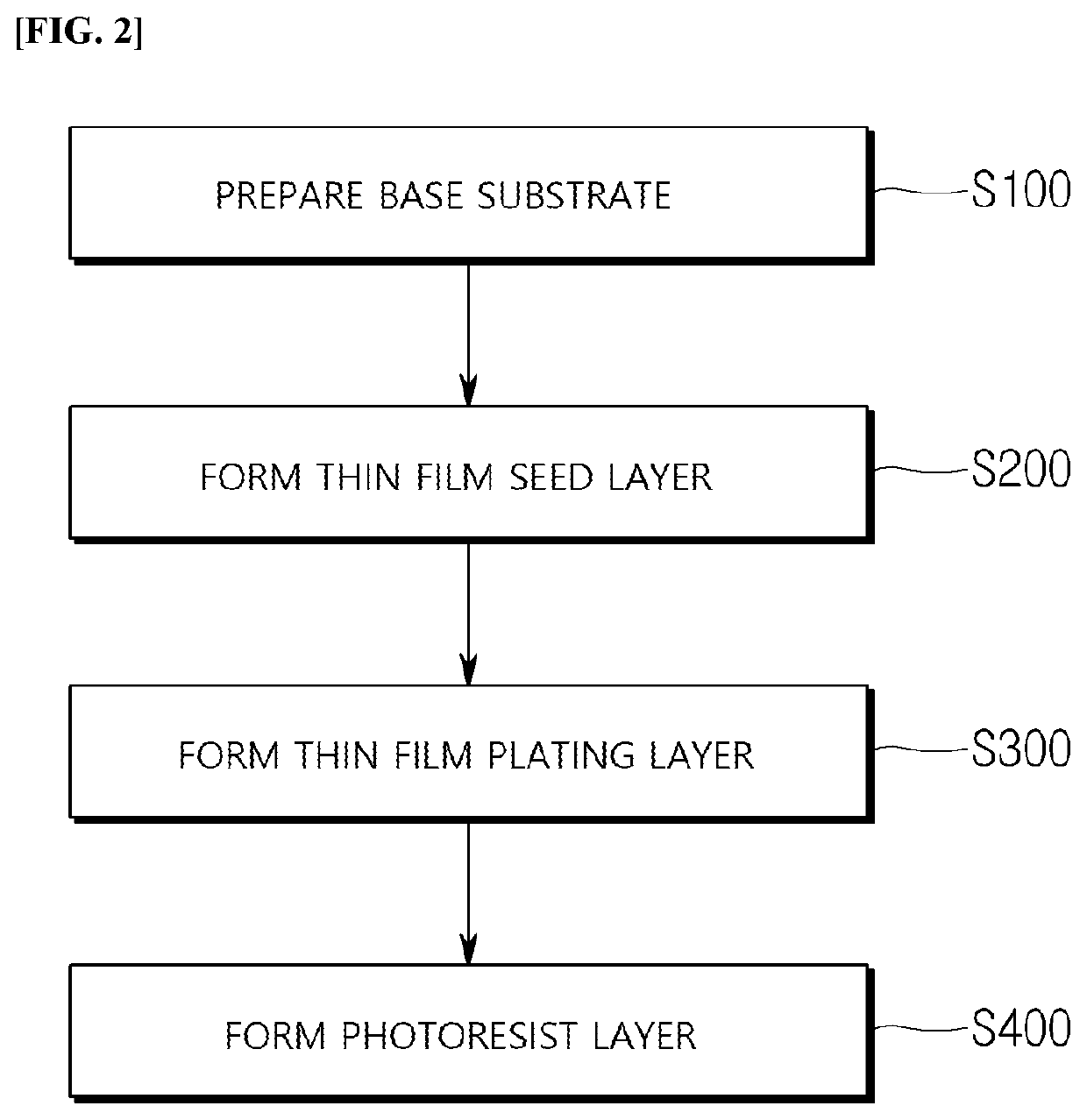
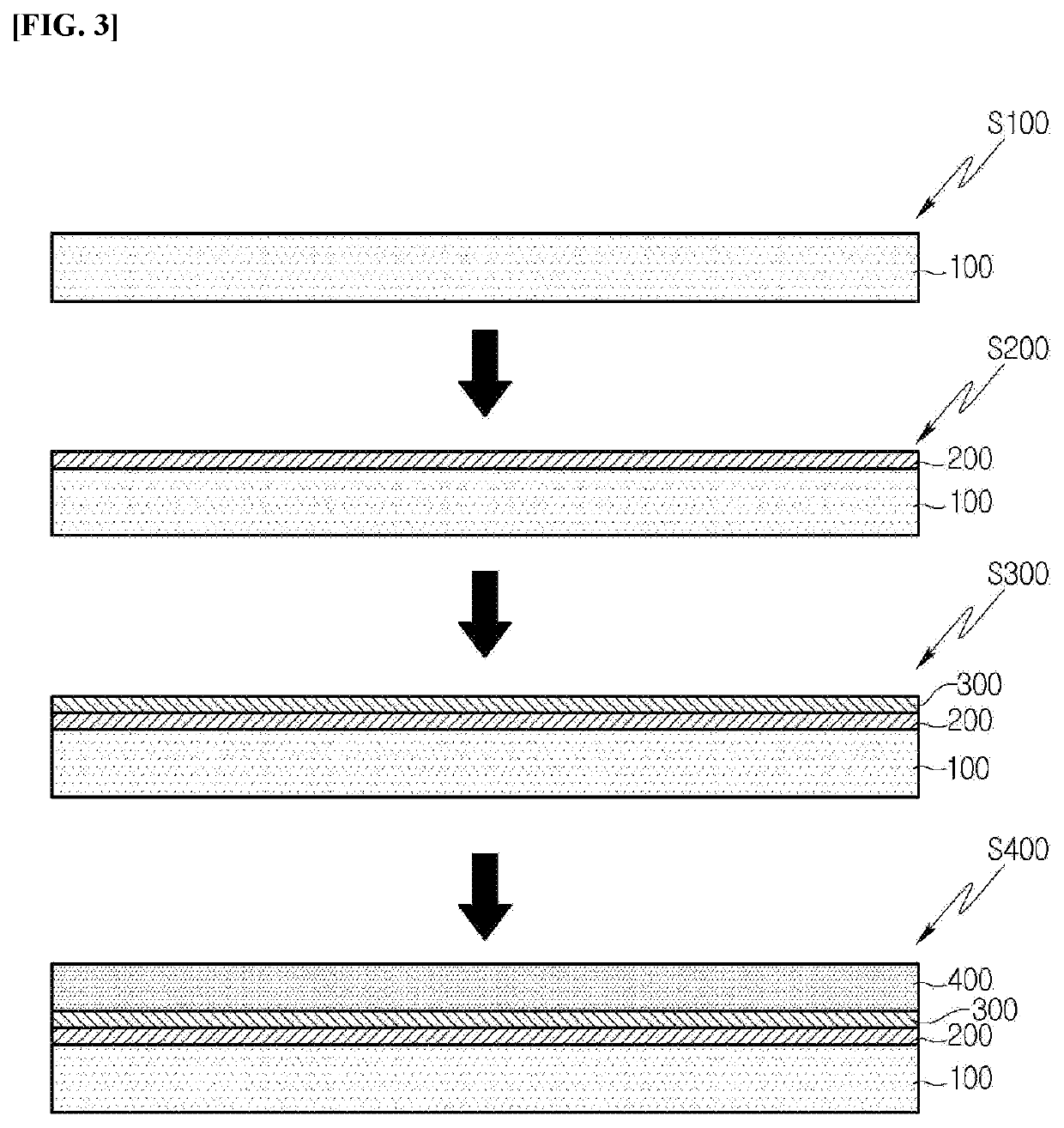
[0013]Hereinafter, the most preferred embodiment of the present disclosure will be described with reference to the accompanying drawings in order to specifically describe so that those skilled in the art to which the present disclosure pertains may easily practice the technical spirit of the present disclosure. First, in adding reference numerals to the components of each drawing, it should be noted that the same components are denoted by the same reference numerals as much as possible even if displayed on different drawings. In addition, in describing the present disclosure, when it is determined that the detailed description of the related known configuration or function may obscure the gist of the present disclosure, the detailed description thereof will be omitted.

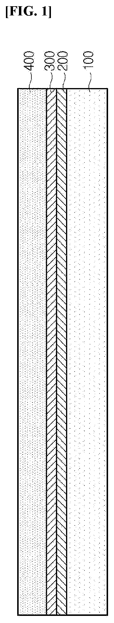
[0014]Referring to FIG. 1, a thin film circuit substrate according to an embodiment of the present disclosure includes a base substrate 100, a thin film seed layer 200, a thin film plating layer 300, and a pho...


PUM


Abstract

Disclosed is a thin film circuit substrate and a manufacturing method thereof, which are capable of forming a pattern having a feature size of less than 10 μm by forming a seed layer and a plating layer on a base substrate and then forming, through electrospinning, a photoresist layer having a thickness in a set range. The disclosed thin film circuit substrate comprises: a base substrate; a thin film seed layer formed on the top surface of the base substrate; a metal layer formed on the top surface of the thin film seed layer; and a photoresist layer formed on the top surface of the metal layer, wherein the thickness of the photoresist layer is in a range of 1 μm to 5 μm.

Description

TECHNICAL FIELD[0001]The present disclosure relates to a thin film circuit substrate and a manufacturing method thereof, and more particularly, to a thin film circuit substrate used for manufacturing a film of a Chip On Film (COF) requiring a fine circuit pattern and a manufacturing method thereof.BACKGROUND ART[0002]A Chip On Film (COF) is a method of mounting a semiconductor chip on a thin film-shaped printed circuit substrate (PCB). The COF may form a pattern having a thinner line width as compared to a Tape Carrier Package (TCP).[0003]Recently, the demand for the COF capable of a fine pattern is rapidly increasing according to the trend of the light, thin, short, and small form of a portable terminal. The thin film circuit substrate (or thin film) for the COF may form the pattern having the line width of about 10 μm.[0004]However, with the lighter, thinner, shorter, and smaller trend of the portable terminal, a pattern having a thinner line width is required.[0005]According to t...

Claims


Application Information

Patent Timeline
IPC IPC(8): G03F7/11H05K1/09H05K3/06
CPCH05K3/064H05K1/09G03F7/11G03F7/164H05K3/022H05K1/0393H05K3/025G03F7/004
Inventor DAN, SUNG-BAEK
Owner AMOGREENTECH CO LTD
Why Eureka
Try Eureka