Light-Emitting Element, Display Device, Electronic Device, and Lighting Device

a technology of light-emitting elements and electronic devices, which is applied in the direction of luminescent compositions, organic semiconductor devices, chemistry apparatuses and processes, etc., can solve the problems of difficult to achieve high reliability of fluorescent light-emitting elements, high emission efficiency, and low driving voltag

Active Publication Date: 2020-10-29
SEMICON ENERGY LAB CO LTD
View PDF6 Cites 4 Cited by
  • Summary
  • Abstract
  • Description
  • Claims
  • Application Information

AI Technical Summary

Benefits of technology

[0032]One embodiment of the present invention can provide a light-emitting element having high emission efficiency. Another embodiment of the present invention can provide a light-emitting element with low driving voltage. Another embodiment of the present invention can provide a highly reliable light-emitting element. Another embodiment of the present invention can provide a light-emitting element with low power consumption. Another embodiment of the present invention can provide a light-emitting element that emits light with high color purity. Another embodiment of the present invention can provide a novel light-emitting element. Another embodiment of the present invention can provide a novel light-emitting device. Another embodiment of the present invention can provide a novel electronic device.

Problems solved by technology

Thus, a fluorescent light-emitting element is likely to have lower emission efficiency than a phosphorescent light-emitting element.
In addition, a fluorescent light-emitting element requires a large amount of current to emit light with high luminance and thus the amounts of generated heat and current load become higher.
Accordingly, it is difficult for a fluorescent light-emitting element to have high reliability.

Method used


Image

  • Light-Emitting Element, Display Device, Electronic Device, and Lighting Device
  • Light-Emitting Element, Display Device, Electronic Device, and Lighting Device
  • Light-Emitting Element, Display Device, Electronic Device, and Lighting Device

Examples


embodiment 1

[0094]In this embodiment, a light-emitting element of one embodiment of the present invention will be described below with reference to FIGS. 1A to 1C, FIGS. 2A and 2B, FIG. 3, and FIGS. 4A and 4B.

Structure Example 1 of Light-Emitting Element

[0095]First, the structure of the light-emitting element of one embodiment of the present invention will be described below with reference to FIGS. 1A to 1C.

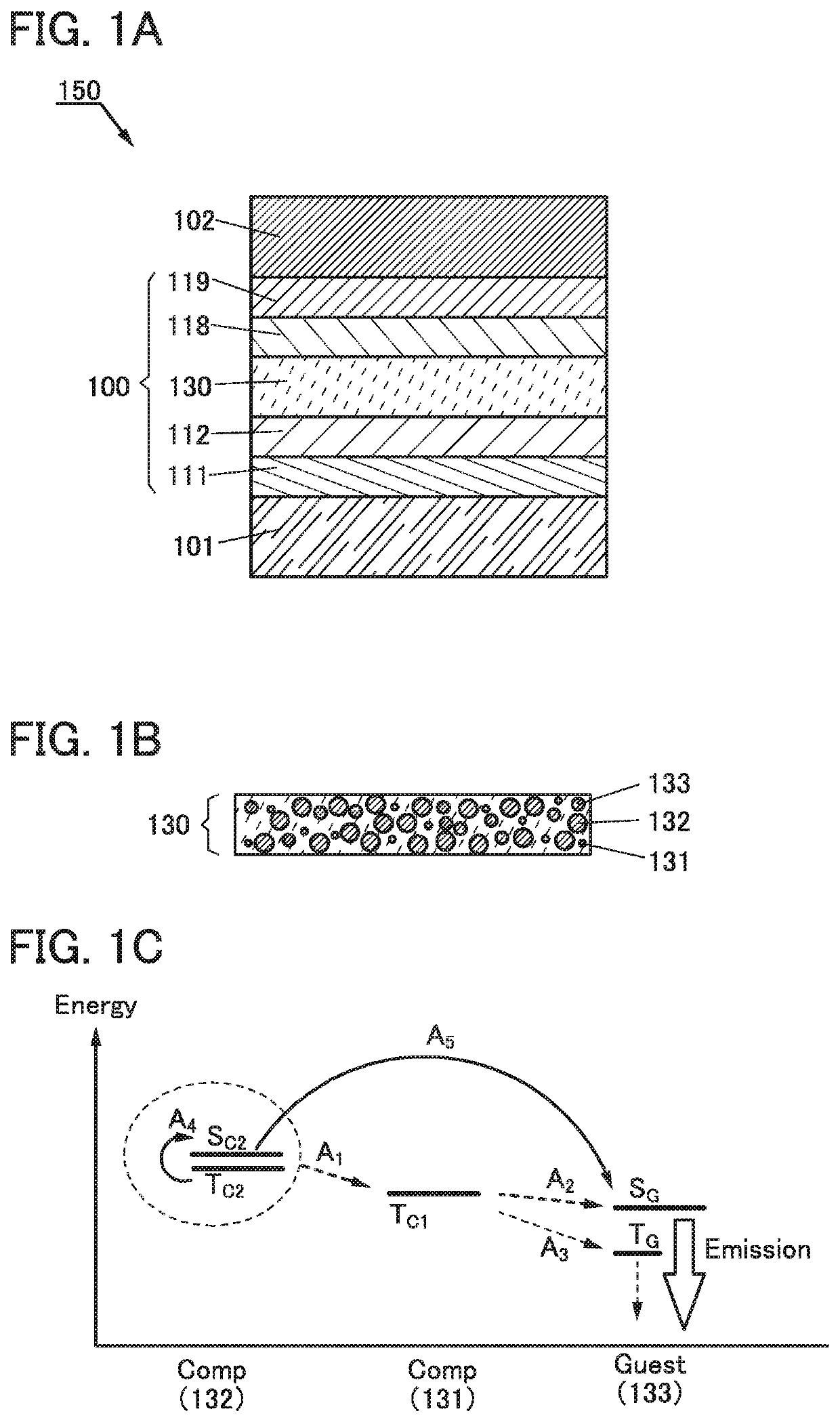
[0096]FIG. 1A is a schematic cross-sectional view of a light-emitting element 150 of one embodiment of the present invention.

[0097]The light-emitting element 150 includes a pair of electrodes (an electrode 101 and an electrode 102) and an EL layer 100 between the pair of electrodes. The EL layer 100 includes at least a light-emitting layer 130.

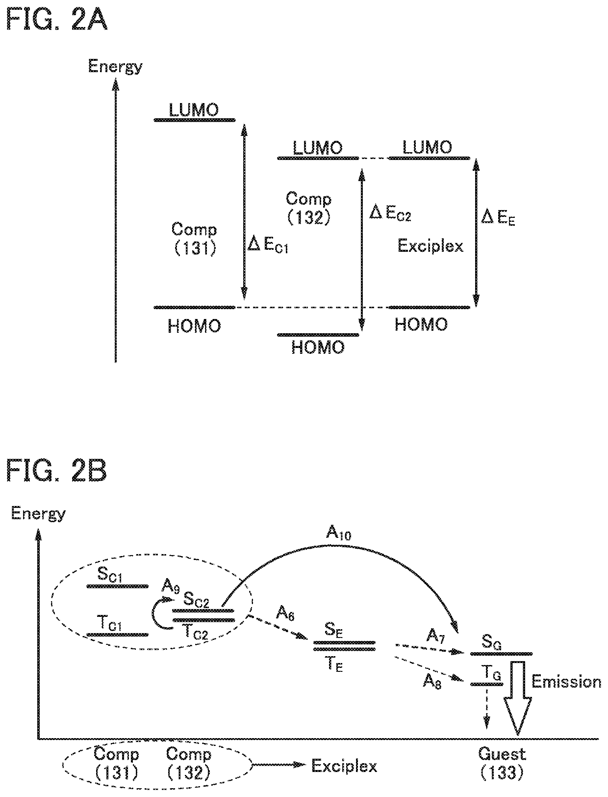
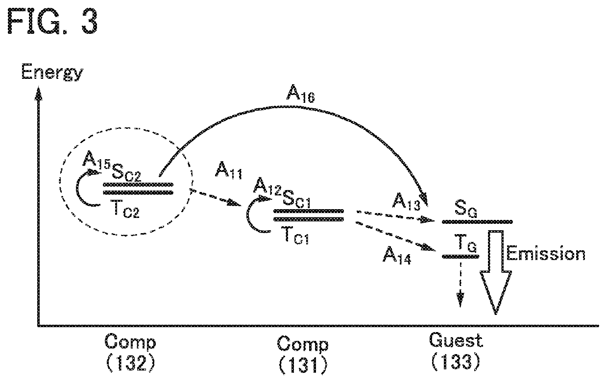
[0098]The EL layer 100 illustrated in FIG. 1A includes functional layers such as a hole-injection layer 111, a hole-transport layer 112, an electron-transport layer 118, and an electron-injection layer 119, in addition to the light-emitting layer 130.

[...

embodiment 2

[0259]In this embodiment, a light-emitting element having a structure different from that described in Embodiment 1 will be described below with reference to FIG. 5. In FIG. 5, a portion having a function similar to that in FIG. 1A is represented by the same hatch pattern as in FIG. 1A and not particularly denoted by a reference numeral in some cases. In addition, common reference numerals are used for portions having similar functions, and a detailed description of the portions is omitted in some cases.

Structure Example 2 of Light-Emitting Element

[0260]FIG. 5 is a schematic cross-sectional view of a light-emitting element 250.

[0261]The light-emitting element 250 illustrated in FIG. 5 includes a plurality of light-emitting units (a light-emitting unit 106 and a light-emitting unit 108) between the pair of electrodes (the electrode 101 and the electrode 102). One of the light-emitting units preferably has the same structure as the EL layer 100 illustrated in FIG. 1A. That is, it is p...

embodiment 3

[0279]In this embodiment, a light-emitting device including the light-emitting element described in Embodiment 1 and Embodiment 2 is described with reference to FIGS. 6A and 6B.

[0280]FIG. 6A is a top view of the light-emitting device and FIG. 6B is a cross-sectional view taken along the lines A-B and C-D in FIG. 6A. The light-emitting device includes a driver circuit portion (source side driver circuit) 601, a pixel portion 602, and a driver circuit portion (gate side driver circuit) 603, which control light emission of a light-emitting element and are illustrated with dotted lines. Moreover, a reference numeral 604 denotes a sealing substrate, a reference numeral 625 denotes a desiccant, and a reference numeral 605 denotes a sealant. A portion surrounded by the sealant 605 is a space 607.

[0281]Note that a lead wiring 608 is a wiring for transmitting signals to be input to the source side driver circuit 601 and the gate side driver circuit 603 and for receiving a video signal, a clo...


PUM

PropertyMeasurementUnit
triplet excitation energy levelaaaaaaaaaa
singlet excitation energyaaaaaaaaaa
temperatureaaaaaaaaaa

Abstract

A light-emitting element having high emission efficiency is provided.
The light-emitting element includes a first organic compound, a second organic compound, and a third organic compound. The first organic compound has a function of converting triplet excitation energy into light emission. The second organic compound is preferably a TADF material. The third organic compound is a fluorescent compound. Light emitted from the light-emitting element is obtained from the third organic compound. Triplet excitation energy in a light-emitting layer is transferred to the third organic compound by reverse intersystem crossing caused by the second organic compound or through the first organic compound.

Description

TECHNICAL FIELD[0001]One embodiment of the present invention relates to a light-emitting element, or a display device, an electronic device, and a lighting device each including the light-emitting element.[0002]Note that one embodiment of the present invention is not limited to the above technical field. The technical field of one embodiment of the invention disclosed in this specification and the like relates to an object, a method, or a manufacturing method. In addition, one embodiment of the present invention relates to a process, a machine, manufacture, or a composition of matter. Specifically, examples of the technical field of one embodiment of the present invention disclosed in this specification include a semiconductor device, a display device, a liquid crystal display device, a light-emitting device, a lighting device, a power storage device, a memory device, a method for driving any of them, and a method for manufacturing any of them.BACKGROUND ART[0003]In recent years, re...

Claims


Application Information

Patent Timeline
Patent Type & Authority Applications(United States)
IPC IPC(8): H01L51/50C09K11/06C09K11/02
CPCH01L51/0052H01L51/5028H01L51/0072H01L27/3244C09K11/06H01L2251/5376H01L51/5278H01L51/0071H01L51/0074H01L51/5072H01L51/0067C09K2211/1044H01L51/0085H01L2251/552H01L51/0054H01L51/0061C09K11/02H01L51/5044C09K2211/185C09K2211/1007H01L51/005H01L51/0058H01L27/323H10K85/636H10K85/654H10K85/6576H10K85/6572H10K85/342H10K50/12H10K50/11H10K2101/10H10K2101/20H05B33/02H10K59/00H10K50/84H10K50/121H10K50/16H10K50/19H10K50/131H10K59/12H10K59/40H10K85/60H10K85/615H10K85/622H10K85/626H10K85/657H10K2101/27H10K2101/30
Inventor OHSAWA, NOBUHARUSEO, SATOSHI
Owner SEMICON ENERGY LAB CO LTD
Why Eureka
Try Eureka