
Three-Dimensional Processor for Parallel Computing

a three-dimensional processor and parallel computing technology, applied in the field of integrated circuits, can solve the problems of computational difficulty, non-arithmetic functions cannot be implemented by the conventional logic circuit alone, and non-arithmetic functions cannot be realized by the conventional logic circuit, so as to achieve non-arithmetic functions quickly and efficiently, improve computational complexity, and improve computational efficiency

Pending Publication Date: 2020-11-12
HANGZHOU HAICUN INFORMATION TECH
View PDF0 Cites 0 Cited by
  • Summary
  • Abstract
  • Description
  • Claims
  • Application Information

AI Technical Summary

Benefits of technology

The present invention is about a three-dimensional processor for parallel computing. It includes a semiconductor substrate and a plurality of computing elements. Each computing element has a three-dimensional memory array and an arithmetic logic circuit. The memory array stores a portion of a look-up table for a mathematical function, while the arithmetic logic circuit performs arithmetic operations on the data stored in the memory array. The processor also has a plurality of inter-storage-processor connections that connect the memory array and the substrate. The invention provides a three-dimensional processor that is smaller and faster than conventional processors, and it can perform more complex functions with a smaller footprint. The invention also allows for the flattening of the scientific computation framework and the rapid and efficient computation of mathematical models.

Problems solved by technology

However, the conventional logic circuits are not suitable for non-arithmetic functions, whose operations include more than the basic arithmetic operations.
Because they cannot be represented by a combination of the basic arithmetic operations, the non-arithmetic functions cannot be implemented by the conventional logic circuits alone.
Non-arithmetic functions are computationally hard and their hardware implementation has been a major challenge.
The 2-D integration severely limits computational density and computational complexity.
This has an adverse effect on parallel computation.
Apparently, the software-implemented functions (e.g. mathematical functions, mathematical models) run much slower and less efficient than the hardware-implemented functions (i.e. built-in functions), and extra software-decomposition steps (e.g. for mathematical models) would make these performance gaps even more pronounced.
Typical mathematical models are nonlinear and cannot be represented by a combination of these arithmetic operations.
This large amount of computation makes simulation extremely slow and inefficient.
Because the non-single-crystalline (e.g. polycrystalline or amorphous) semiconductor materials are inferior in performance than the single-crystalline semiconductor materials, a 3D-M cell is generally slower in speed than a 2D-M cell.
Accordingly, although it has a larger storage capacity, the 3D-M was considered not suitable for high-performance computation (HPC), e.g. as an embedded memory in a high-speed processor.

Method used


Image

  • Three-Dimensional Processor for Parallel Computing
  • Three-Dimensional Processor for Parallel Computing
  • Three-Dimensional Processor for Parallel Computing

Examples


Embodiment Construction

[0041]Those of ordinary skills in the art will realize that the following description of the present invention is illustrative only and is not intended to be in any way limiting. Other embodiments of the invention will readily suggest themselves to such skilled persons from an examination of the within disclosure.

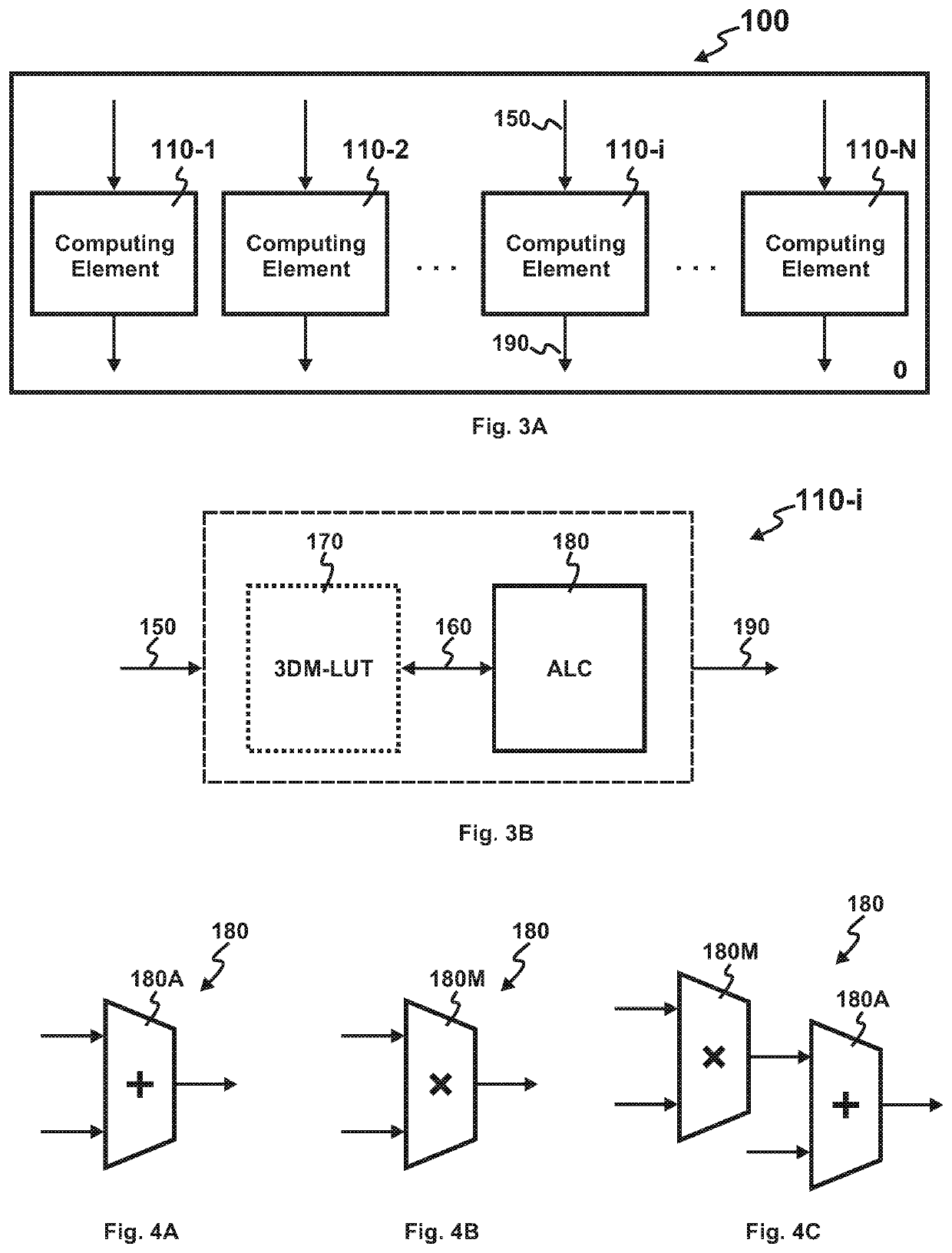
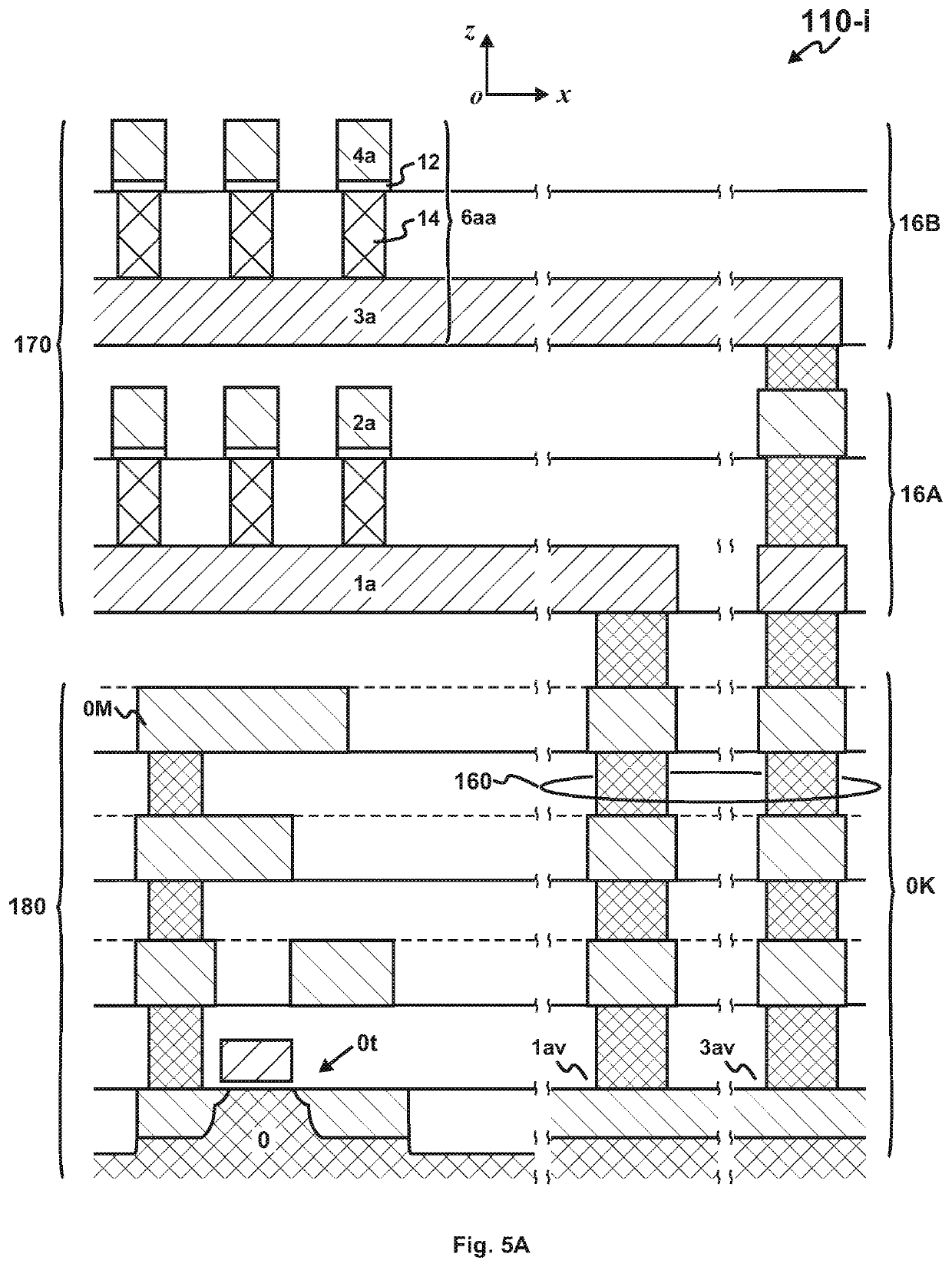
[0042]Referring now to FIG. 3A-3B, a preferred three-dimensional processor (3D-processor) 100 is disclosed. It comprises a semiconductor substrate 0 and an array of computing elements 110-1, 110-2 . . . 110-i . . . 110-N formed thereon (FIG. 3A). These computing elements 110-1 . . . 110-N could realize a same function or different functions. Each computing element 110-i has one or more input variables 150, and one or more output variables 190 (FIG. 3B). It further comprises at least a three-dimensional memory (3D-M) array 170 for storing at least a portion of the 3DM-LUT for a mathematical function and an arithmetic logic circuit (ALC) 180 for performing arithmetic operatio...


PUM


Abstract

A three-dimensional processor (3D-processor) for parallel computing includes a plurality of computing elements. Each computing element comprises at least a three-dimensional memory (3D-M) array for storing at least a portion of a look-up table (LUT) for a mathematical function and an arithmetic logic circuit (ALC) for performing arithmetic operations on the LUT data. Deficiency in latency is offset by a large scale of parallelism.

Description

CROSS-REFERENCE TO RELATED APPLICATIONS[0001]This application is a continuation-in-part of U.S. patent application Ser. No. 15 / 487,366, filed Apr. 13, 2017. This application is further a continuation-in-part of U.S. patent application Ser. No. 16 / 458,187, filed Jun. 30, 2019, which is also a continuation-in-part of U.S. patent application Ser. No. 15 / 487,366, filed Apr. 13, 2017.[0002]These applications claim priorities from Chinese Patent Application 201610083747.7, filed on Feb. 13, 2016; Chinese Patent Application 201610260845.3, filed on Apr. 22, 2016; Chinese Patent Application 201610289592.2, filed on May 2, 2016; Chinese Patent Application 201710237780.5, filed on Apr. 12, 2017, in the State Intellectual Property Office of the People's Republic of China (CN), the disclosure of which are incorporated herein by references in their entireties.BACKGROUND1. Technical Field of the Invention[0003]The present invention relates to the field of integrated circuit, and more particularly...

Claims


Application Information

Patent Timeline
Patent Type & Authority Applications(United States)
IPC IPC(8): G06F7/57G06F7/544G06F9/30G06F16/901G06F9/38H01L27/11556H10B41/27
CPCG06F16/9017H01L27/11556G06F9/3001G06F9/3877G06F7/544G06F7/57H10B41/27
Inventor ZHANG, GUOBIAOSHEN, CHEN
Owner HANGZHOU HAICUN INFORMATION TECH
Learn More