Reconstituted substrate for radio frequency applications

a radio frequency application and substrate technology, applied in the direction of solid-state devices, semiconductor/solid-state device details, printed circuit manufacturing, etc., can solve the problems of reducing radiation efficiency, increasing the complexity of 2d and 3d structures, and limited bandwidth of antennas assembled in close proximity thereto

Active Publication Date: 2020-11-12
APPLIED MATERIALS INC
View PDF0 Cites 21 Cited by
  • Summary
  • Abstract
  • Description
  • Claims
  • Application Information

AI Technical Summary

Problems solved by technology

As wireless technology advances, these structures are evolving into increasingly complex 2D and 3D structures with millions of transistors, capacitors, and resisters integrated therein an in close proximity to each other and the assembled antenna systems.
However, these conventional semiconductor materials are characterized by increased dissipation of electromagnetic energy, resulting in reduced radiation efficiency and limited bandwidth of antennas assembled in close proximity thereto.
The lossy nature of conventional semiconductor materials is particularly evident when utilizing high frequency (HF) antenna systems for high frequency applications.

Method used


Image

  • Reconstituted substrate for radio frequency applications
  • Reconstituted substrate for radio frequency applications
  • Reconstituted substrate for radio frequency applications

Examples


Embodiment Construction

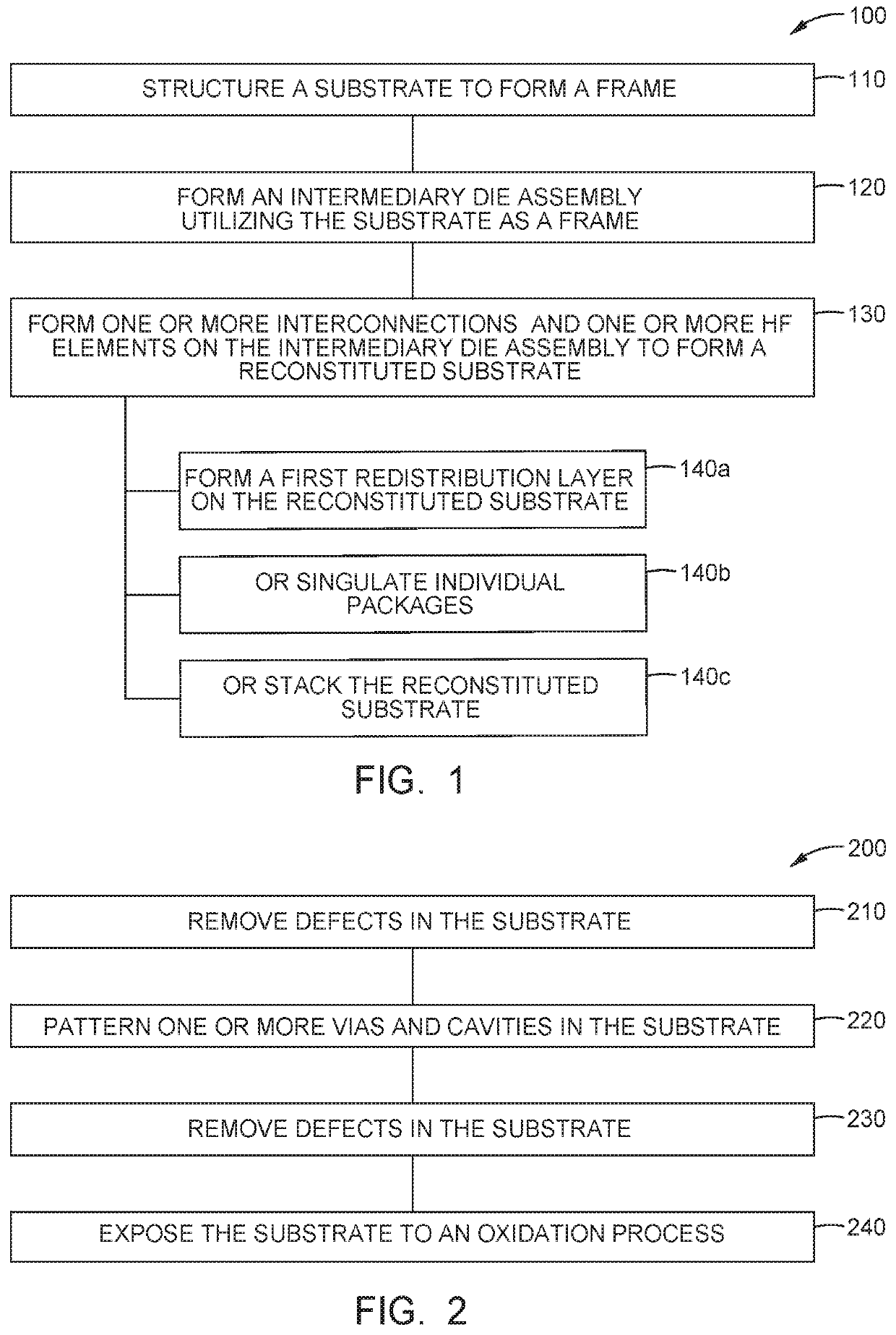
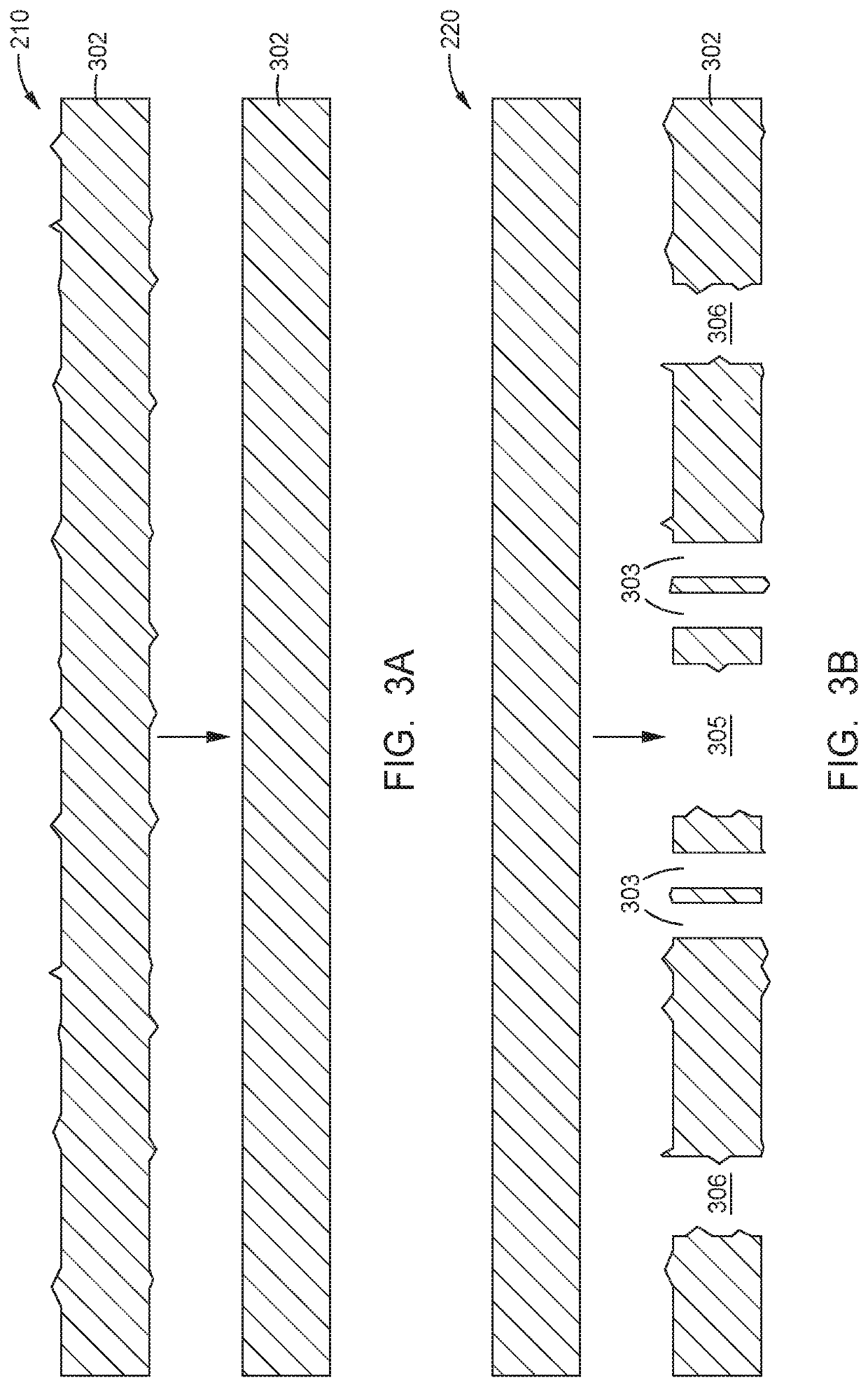
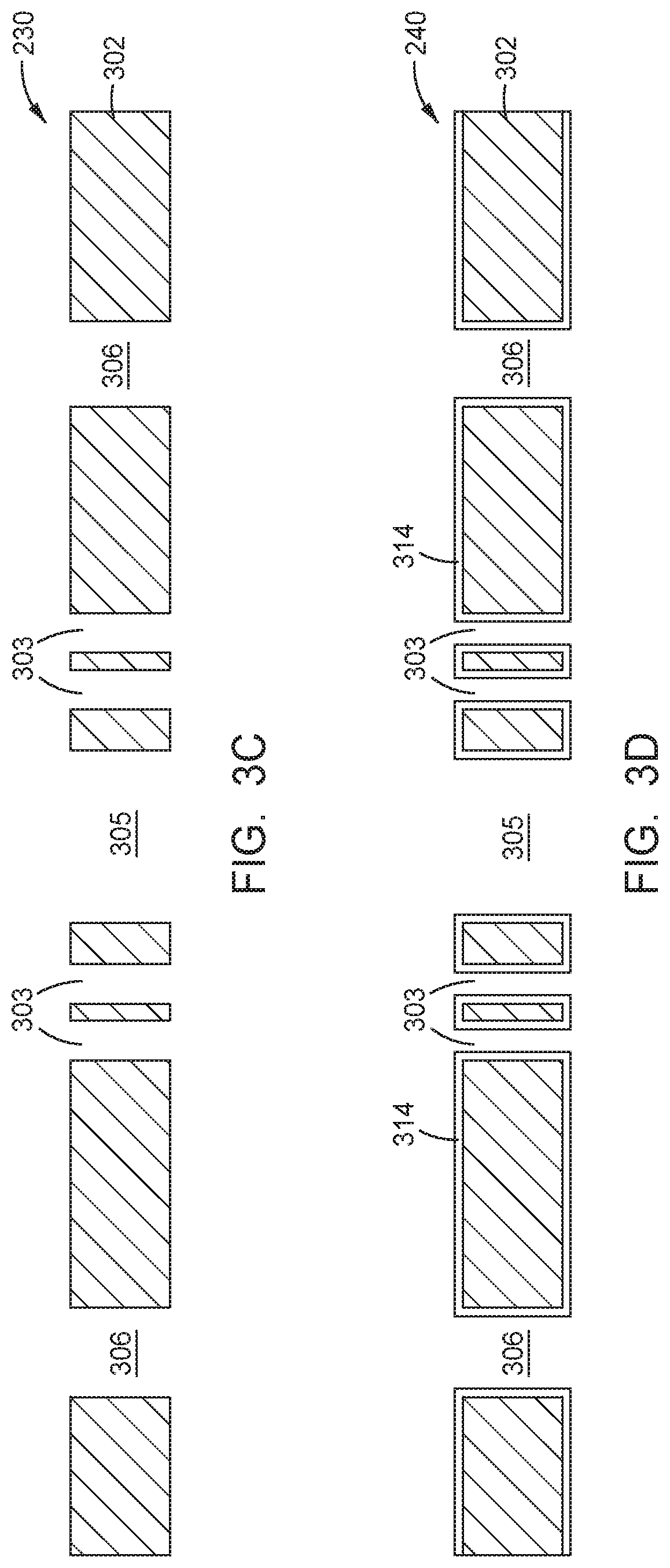
[0021]The present disclosure relates to methods and apparatus for forming thin-form-factor reconstituted substrates and semiconductor device packages for high frequency applications. The substrate and package structures described herein may be utilized in high-density 2D and 3D integrated devices for 4G, 5G, 6G, and other wireless network systems. In one embodiment, a silicon substrate is structured by laser ablation to include cavities for placement of semiconductor dies and vias for deposition of conductive interconnections. Additionally, one or more cavities are structured to be filled or occupied with a flowable dielectric material. Integration of one or more high frequency components adjacent the dielectric-filled cavities enables improved performance of the radio frequency (“RF”) elements with reduced signal loss caused by the silicon substrate.

[0022]FIG. 1 illustrates a flow diagram of a representative method 100 of forming a reconstituted substrate, which may be homogeneous ...


PUM

PropertyMeasurementUnit
thicknessaaaaaaaaaa
thicknessaaaaaaaaaa
diameteraaaaaaaaaa

Abstract

The present disclosure relates to methods and apparatus for forming thin-form-factor reconstituted substrates and semiconductor device packages for radio frequency applications. The substrate and package structures described herein may be utilized in high-density 2D and 3D integrated devices for 4G, 5G, 6G, and other wireless network systems. In one embodiment, a silicon substrate is structured by laser ablation to include cavities for placement of semiconductor dies and vias for deposition of conductive interconnections. Additionally, one or more cavities are structured to be filled or occupied with a flowable dielectric material. Integration of one or more radio frequency components adjacent the dielectric-filled cavities enables improved performance of the radio frequency elements with reduced signal loss caused by the silicon substrate.

Description

CROSS-REFERENCE TO RELATED APPLICATIONS[0001]This application claims benefit of priority to Italian patent application number 102019000006736, filed May 10, 2019, which is herein incorporated by reference in its entirety.BACKGROUNDField[0002]Embodiments of the present disclosure generally relate to the field of semiconductor device manufacturing, and more particularly, to structures and methods of packaging semiconductor devices.Description of the Related Art[0003]In wireless networks such as mobile communication networks, connectivity and communication between devices is achieved through the utilization of miniaturized antenna systems having antennas in combination with other electrical elements such as receivers or transmitters. Recently, the demand for increased data transfer rates of wireless networks has led to the development of 5G and 6G technologies utilizing new radio frequency (RF) bands, which has imposed stringent specifications on the design of RF antennas and other cor...

Claims


Application Information

Patent Timeline
Patent Type & Authority Applications(United States)
IPC IPC(8): H01Q1/24H01Q1/22H05K1/02H01L23/66H01L23/538
CPCH01L23/66H01Q1/243H01L23/5386H01L23/5384H05K1/0243H01Q1/2283H01L23/49827H01L23/5389H01L21/486H01L21/4864H01L25/0657H01L21/50H01L21/4846H01L23/49838H01L23/5385H01L23/49866H01L23/49894H01L23/147H01L23/15H01L2224/18H01L2224/04105H01L2224/73267H01L2224/92244H01L25/105H01L2225/1035H01L2225/1058H01L2225/1088H05K2203/1476H05K1/185H05K3/4007H05K3/107H05K3/4623H05K3/4673H01L24/19H01L24/20H01L24/97H01L2224/32145H01L24/96H01L24/32H01L24/73H01L23/28H01L23/13H01L2225/107H01L21/76802H01L27/0688H01L2021/60007
Inventor SEE, GUAN HUEICHIDAMBARAM, RAMESH
Owner APPLIED MATERIALS INC
Why Eureka
Try Eureka