
Manufacturing method of mounting structure

Active Publication Date: 2020-12-10
NAGASE CHEMTEX CORPORATION
View PDF0 Cites 2 Cited by
  • Summary
  • Abstract
  • Description
  • Claims
  • Application Information

AI Technical Summary

Benefits of technology

The present invention provides a way to seal multiple circuit members that have hollow spaces inside them. This helps to maintain the internal spaces of the circuit members, which can be useful in various applications.

Problems solved by technology

Furthermore, with recent miniaturization of electronic devices, circuit boards have been required to be miniaturized, and the distance between the circuit members (including a hollow member) placed on a circuit board has been getting smaller.

Method used


Image

  • Manufacturing method of mounting structure
  • Manufacturing method of mounting structure
  • Manufacturing method of mounting structure

Examples


example 1

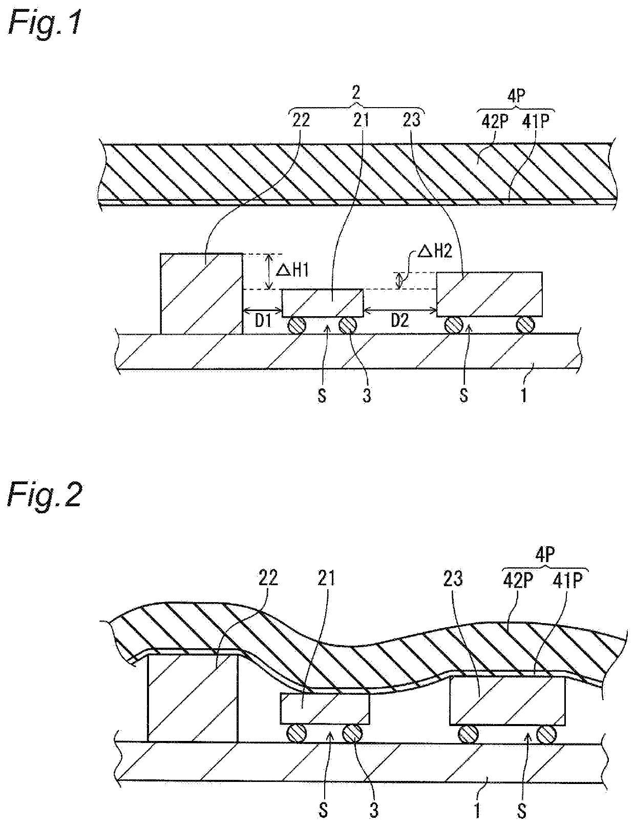
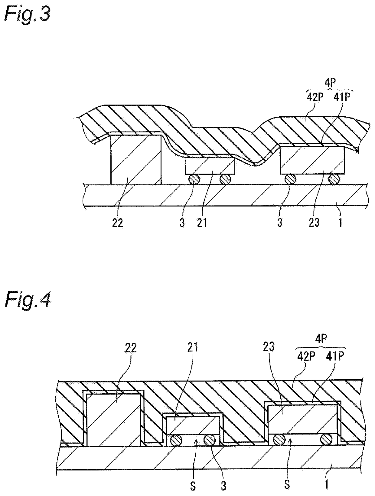
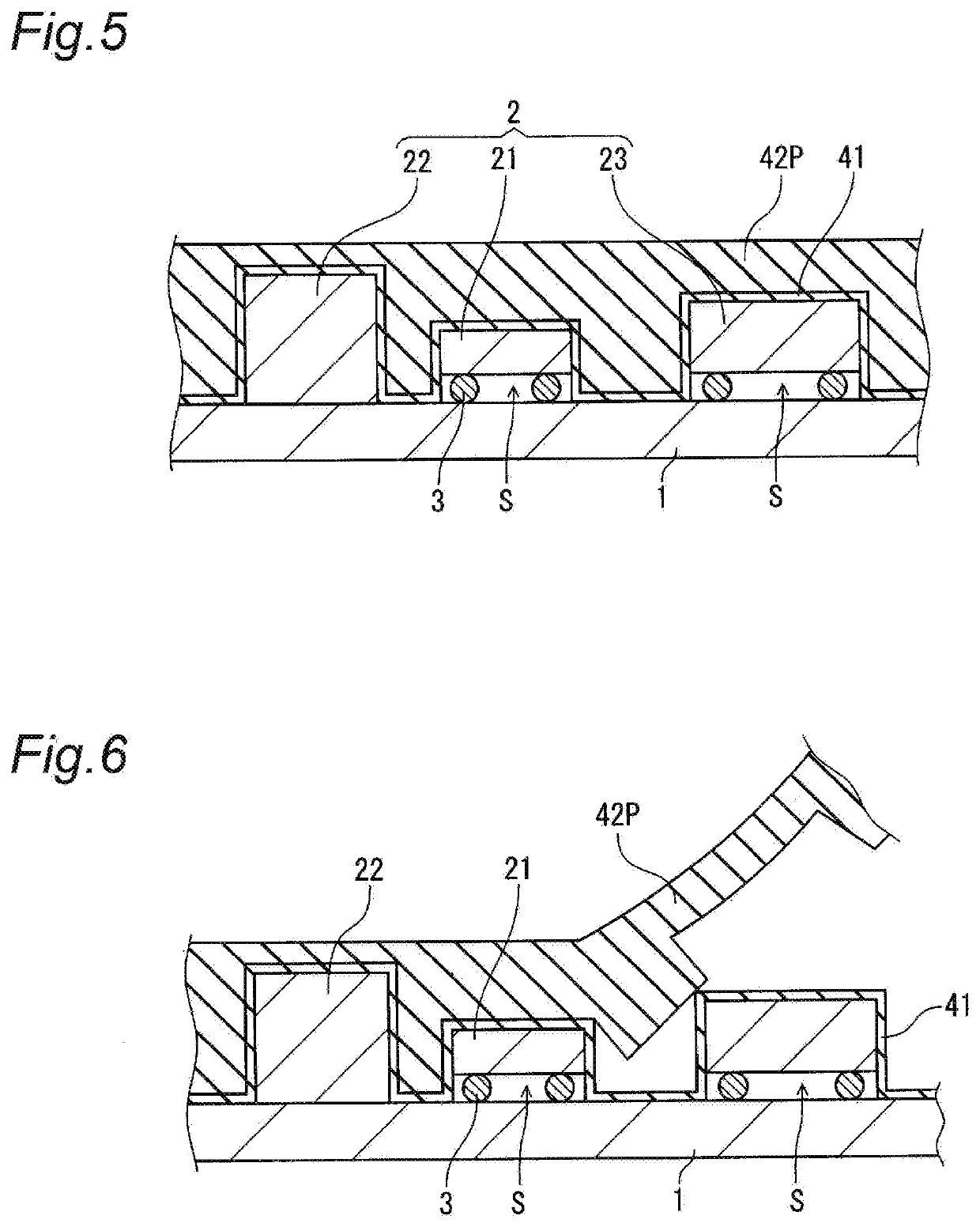
[0147]On a glass epoxy substrate (first circuit member, 50 mm square, thickness: 0.2 mm), the same type of four SAW chips A, B, C and D (second circuit member, 1.1 mm×1.1 mm, height: 0.2 mm) were placed in line, with gold bumps (each 100 μm in diameter and 20 μm in height) interposed therebetween, to form a mounting member. A separation distance D1 between the SAW chips A and B was 0.4 mm, a separation distance D2 between the SAW chips B and C was 0.1 mm, and a separation distance D3 between the SAW chips C and D was 0.2 mm. The mounting member was sealed with a sheet stack (a stack of a thermosetting sheet (first layer) and a thermoplastic sheet (second layer)). In a sealing step, with the sheet stack disposed such that the surface of the thermosetting sheet (first layer) came in contact with the second circuit member side, the sheet stack was pressed under heating at 120° C. (sealing temperature), for 1 min under a reduced pressure atmosphere (200 Pa). This was followed by heating...

reference example 1

[0155]A mounting structure was obtained in the same manner as in Example 1, except that a stack of a first layer and a second layer both having thermosetting property was used as the sheet stack, and peeling was not performed after cooling. In the sheet stack, the thermosetting sheet (thickness: 12 μm) as used in Example 1 was used as the first layer, and as the second layer, a thermosetting sheet (thickness: 250 μm) prepared by a coating method using a resin composition containing the components shown in Table 1 at a ratio shown in Table 1 was used. These thermosetting sheets were overlapped with each other, and heat-laminated as in Example 1, to form a sheet stack. Note that the phenoxy resin used in Reference Example 1 was a thermoplastic resin. With respect to the material constituting each of the sheets, its physical property values were measured by the above-described procedures.

>

[0156]Example and Reference Example were evaluated for the following properties.

[0157](1) Sealing ...


PUM


Abstract

A manufacturing method of a mounting structure, the method including a step of preparing a mounting member including a first circuit member and a plurality of second circuit members placed on the first circuit member; a disposing step of disposing a thermosetting sheet and a thermoplastic sheet on the mounting member, with the thermosetting sheet interposed between the thermoplastic sheet and the first circuit member; a first sealing step of pressing a stack of the thermosetting sheet and the thermoplastic sheet against the first circuit member, and heating the stack, to seal the second circuit members and to cure the thermosetting sheet into a first cured layer; a removal step of removing the thermoplastic sheet from the first cured layer; and a coating film formation step of forming a coating film on the first cured layer, after the removal step. At least one of the second circuit members is a hollow member having a space from the first circuit member, and in the first sealing step, the second circuit members are sealed so as to maintain the space.

Description

TECHNICAL FIELD[0001]The present invention relates to a manufacturing method of a mounting structure, specifically to a manufacturing method of a sealed mounting structure.BACKGROUND ART[0002]Some electronic components (circuit members) placed on a circuit board needs a space from the circuit board. One example is a SAW chip used for noise cancellation in cellular phones and other devices. The SAW chip filters a desired frequency by utilizing a surface acoustic wave that propagates on a piezoelectric substrate (piezoelectric body). Therefore, a space is necessary between the electrodes on the piezoelectric body and the circuit board on which the SAW chip is placed. For sealing such a circuit member (hollow member) with a space from the circuit board (internal space), a sheet-form sealing material is sometimes used.[0003]Furthermore, with recent miniaturization of electronic devices, circuit boards have been required to be miniaturized, and the distance between the circuit members (i...

Claims


Application Information

Patent Timeline
IPC IPC(8): H01L21/56H03H3/08H01L23/31H03H9/25H01L23/12
CPCH01L23/12H03H3/08H03H9/25H01L21/56H01L23/31H01L21/568H01L21/561H01L23/3121H01L23/293H01L2924/1461H01L2924/1421H01L2924/19041H01L2924/19105H01L2224/16227H01L2224/16145H01L2224/131H01L2224/13147H01L2224/13144H01L2224/97H01L2224/94H01L2924/3025H01L23/552H03H9/1078H01L2224/16225H01L25/0655H01L25/18H01L25/50H01L2224/13101H01L24/13H01L24/16H03H9/10H01L2924/014H01L2924/00014H01L2224/81H01L23/29H05K1/144H05K3/4632H05K2203/068H05K2203/1147
Inventor NOMURA, EIICHIMIYAMOTO, YUTAKAHASHIMOTO, TAKAYUKI
Owner NAGASE CHEMTEX CORPORATION
Features
  • Generate Ideas
  • Intellectual Property
  • Life Sciences
  • Materials
  • Tech Scout
  • Unparalleled Data Quality
  • Higher Quality Content
  • 60% Fewer Hallucinations
Learn More