Electronic arrangement and method of manufacturing the same

Pending Publication Date: 2020-12-24
SIGNIFY HLDG BV
View PDF0 Cites 2 Cited by
  • Summary
  • Abstract
  • Description
  • Claims
  • Application Information

AI Technical Summary

Benefits of technology

The present invention aims to solve the problems of inconvenience, inefficiency, and high cost associated with current lighting devices. The invention provides a lighting device and a method of manufacturing it that are convenient, efficient, and cost-effective.

Problems solved by technology

It should be noted that light-emitting arrangements comprising a plurality of electronic components (e.g. LEDs) may generate a quick rise of the temperature of the light-emitting arrangement, and the effect of heat may be detrimental to the electronic components.
However, MCPCBs arranged in an array according to the prior art are usually not easily separable.
Furthermore, separated MCPCBs may suffer from problems related to creepage, i.e. current leakage between conductive layers in the PCBs.

Method used


Image

  • Electronic arrangement and method of manufacturing the same
  • Electronic arrangement and method of manufacturing the same
  • Electronic arrangement and method of manufacturing the same

Examples


Embodiment Construction

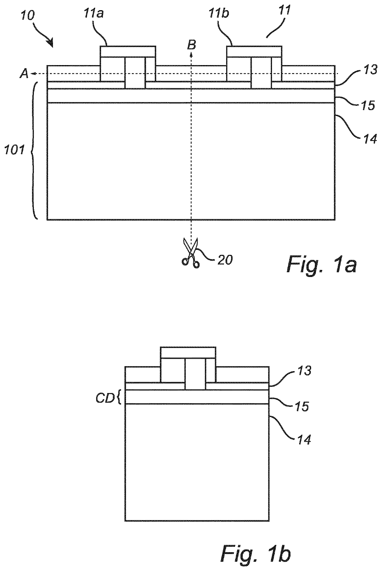
[0041]FIG. 1a is a schematic, cross-sectional view of a metal-core PCB (MCPCB) 10 according to the prior art. The MCPCB 10 comprises a plurality of electronic components 11, which are exemplified as a first LED element 11a and a second LED element 11b. The electronic elements 11 are arranged along a horizontally extending first axis A. The MCPCB 10 further comprises a first metal layer 13 and a second metal layer 14, and a layer 15 which is arranged between the first metal layer 13 and the second metal layer 14.

[0042]The MCPCB 10 may be cut along a second axis B extending perpendicular to the first axis A. The partitioning or cutting of the MCPCB 10 is schematically indicated by the pair of scissors 20, which eventually separates the first LED element 11a and the second LED element 11b of the MCPCB 10. After cutting, the resulting right (or left) hand portion of the MCPCB 10 in FIG. 1a is schematically shown in FIG. 1b. However, the distance CD (which furthermore may be denoted as t...


PUM


Abstract

An electronic arrangement (100) and a method of manufacturing an electronic arrangement are provided. The electronic arrangement comprises an array of electronic components (110) arranged along a first axis, A, and a carrier (120) arranged to support the array of electronic components, wherein the carrier comprises, a first metal layer (130), a second metal layer (140), and an at least partially insulating layer (150) arranged between the first and second metal layers. The electronic arrangement further comprises a partition portion (160) arranged between two adjacently arranged electronic components for partitioning the electronic arrangement, wherein the second metal layer comprises a void (180) intersected by the second axis, wherein the void has a width (190) which extends parallel to the first axis, such that, at the second axis, the second metal layer is undercut with respect to the first metal layer, in a direction parallel to the first axis.

Description

FIELD OF THE INVENTION[0001]The present invention generally relates to the field of electronic arrangements, such as printed circuit boards, and methods of manufacturing such electronic arrangements.BACKGROUND OF THE INVENTION[0002]The use of light-emitting diodes (LED) for illumination purposes continues to attract attention. Compared to incandescent bulbs, LEDs provide numerous advantages such as a longer operational life and an increased efficiency related to the ratio between light energy and heat energy. LED lamps may be used for a general lighting or even for a more specific lighting, as the color and the output power of the LEDs may be tuned.[0003]Many light-emitting arrangements in the prior art, which comprise LEDs, further comprise a printed circuit board (PCB) upon which the LEDs are arranged. The PCB may comprise an electrical insulating layer (e.g. a dielectric layer or a glass fibre-filled epoxy layer) and a metal layer provided below the insulating layer, arranged for...

Claims


Application Information

Patent Timeline
IPC IPC(8): H05K1/18H01L25/075H01L33/62H05K3/34
CPCH05K3/34H01L2933/0066H05K2201/0969H05K2201/0909H05K2201/09972H05K3/0052H05K1/189H05K2201/09036H01L33/647H01L25/0753H01L33/62H05K2201/10106H05K1/0256H05K2201/0761H05K2201/09063H05K2201/10522H05K2203/0228F21S4/24
Inventor LIN, LIHUAOEPTS, WOUTER
Owner SIGNIFY HLDG BV
Why Eureka
Try Eureka