
Lithographically defined vertical interconnect access (VIA) for a bridge die first level interconnect (FLI)

a technology of bridge die and access, which is applied in the field of lithographically defined vertical access (lithovia) for bridge die first level interconnect (fli), can solve the problems of laser drilling techniques that cannot achieve laser drilled vias above the bridge die that are less than 50 m, and the position of the protruded interconnect structure is unsatisfactory,

Pending Publication Date: 2020-12-31
INTEL CORP
View PDF6 Cites 3 Cited by
  • Summary
  • Abstract
  • Description
  • Claims
  • Application Information

AI Technical Summary

Benefits of technology

The patent text describes a technique for creating semiconductor packages with a bridge die first level interconnect (FLI) using litho-vias. The technique addresses challenges related to reliability and mechanical reliability of the laser drilled vias used for forming the FLI. The patent text proposes a solution to address these challenges and provide a more reliable and reliable semiconductor package design.

Problems solved by technology

However, in a semiconductor package that includes a bridge die, due to reliability concerns, the FLIs that couples semiconductor dies to the bridge die need to be positioned directly on the contact pads of the package substrate that are coupled to the bridge die.
As pitches in bridge die architecture scale to less than 50 microns (μm), forming the laser drilled vias above the bridge die is becoming challenging.
For example, laser drilling techniques cannot achieve pitches for laser drilled vias above the bridge die that are less than 50 μm.
For example, unwanted separation or delamination of a protruded interconnect structure positioned in a laser drilled via above a bridge die can occur when the laser drilled via's bottom diameter is below 16 μm.

Method used


Image

  • Lithographically defined vertical interconnect access (VIA) for a bridge die first level interconnect (FLI)
  • Lithographically defined vertical interconnect access (VIA) for a bridge die first level interconnect (FLI)
  • Lithographically defined vertical interconnect access (VIA) for a bridge die first level interconnect (FLI)

Examples


example

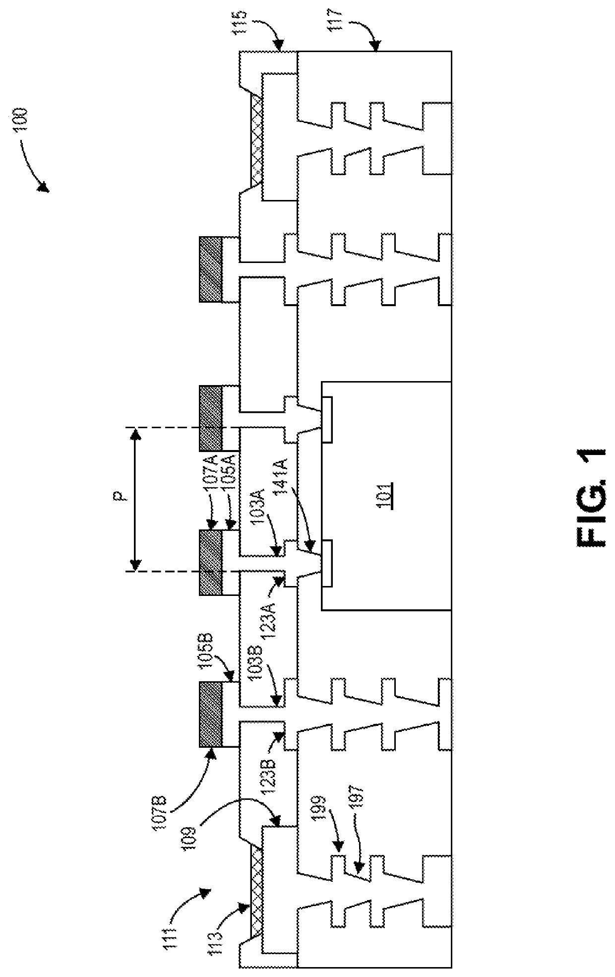
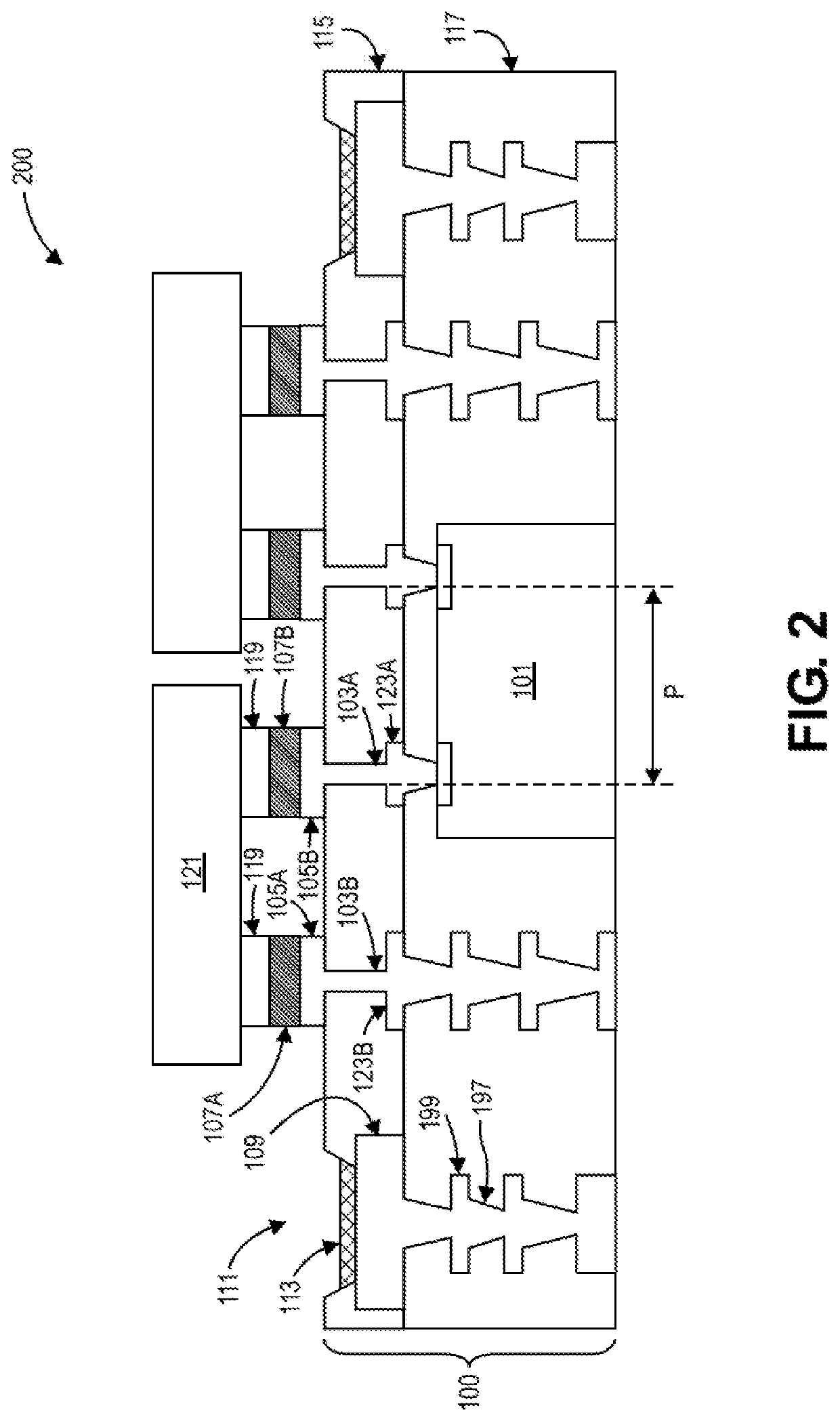
[0044 embodiment 2: The package substrate of example embodiment 1, further comprising: a third contact pad inside the perimeter of the bridge die, adjacent to the second contact pad, and coupled to the bridge die by a second via having substantially vertical sidewalls. The third contact pad has a protruded interconnect structure positioned thereon.

[0045]Example embodiment 3: The package substrate of example embodiment 2, wherein a pitch between the first and second vias is less than or equal to 50 microns (μm).

example embodiment 4

[0046] The package substrate of any one of example embodiments 2-3, further comprising: a dielectric layer surrounding the first and second vias.

example embodiment 5

[0047] The package substrate of any one of example embodiments 2-3, further comprising: a solder resist layer surrounding the first and second vias.

[0048]Example embodiment 6: The package substrate of any one of example embodiments 1-5, wherein the surface finish comprises electroless nickel electroless palladium immersion gold (ENEPIG).


PUM


Abstract

Embodiments described herein relate to lithographically defined vertical interconnect accesses (litho-vias) for a bridge die first level interconnect (FLI) and techniques of fabricating such litho-vias. In one example, a package substrate comprises a bridge die embedded in the package substrate; a first contact pad outside a perimeter of the bridge die; a second contact pad inside the perimeter of the bridge die and coupled to the bridge die by a first via; a third pad inside the perimeter of the bridge die, adjacent to the second contact pad, and coupled to the bridge die by a second via. The first contact pad has a surface finish disposed thereon. A first protruded interconnect structure is positioned on the first via and a second protruded interconnect structure is positioned on the second via. Each of the first and second vias have sidewalls that are substantially vertical.

Description

BACKGROUNDField[0001]Embodiments described herein generally relate to semiconductor packaging. More particularly, embodiments described herein relate to lithographically defined vertical interconnect accesses (litho-vias) for a bridge die first level interconnect (FLI) and techniques of forming such litho-vias.Background Information[0002]A semiconductor package may include one or more semiconductor dies coupled to a package substrate by a first level interconnect (FLI) that comprises protruded interconnect structures (e.g., pillars, bumps, etc.). For example, an FLI couples contact pads of one or more semiconductor dies to contact pads of a package substrate. A semiconductor package may also include a bridge die, which is comprised of routing layers, embedded in a package substrate. The bridge die electrically couples semiconductor dies on the package substrate via an FLI. For example, an FLI couples contact pads of multiple semiconductor dies on a package substrate to contact pads ...

Claims


Application Information

Patent Timeline
IPC IPC(8): H01L23/538H01L21/768H01L23/00
CPCH01L23/5381H01L23/5384H01L21/76897H01L24/06H01L23/5386H01L23/49822H01L23/49827H01L24/16H01L23/49811H01L21/4853H01L21/4857H01L21/486H01L24/81H05K1/181H01L2224/16148H01L2224/16165H01L23/5385H01L23/5383H01L23/49816H01L2224/81192H01L2224/16238H01L2924/15331H01L25/0655H01L24/13
Inventor DARMAWIKARTA, KRISTOFIBRAHIM, TAREKALUR, SIDDHARTHJAIN, RAHULCHEN, HAOBO
Owner INTEL CORP
Learn More