Thermal dissipation structure for integrated circuits

Active Publication Date: 2021-01-14
NATIONAL CHIAO TUNG UNIVERSITY
View PDF0 Cites 0 Cited by
  • Summary
  • Abstract
  • Description
  • Claims
  • Application Information

AI Technical Summary

Benefits of technology

[0013]In summary, according to one or more embodiments of the present disclosure, the thermal dissipation structure is within the semiconductor substrate with integrated circuits to define a thermal dissipation channel, and the distance between the integrated circuits and the thermal dissipation channel is minimized. The heat transfer fluid can flow through the heat dissipation channel, so that the heat of the integrated circuit can be transferred to the heat transfer fluid. When the heat trans

Problems solved by technology

As the semiconductor industry moves to the limit of Moore's Law, conventional semiconductor integrated circuits encounter bottlenecks in development.
Otherwise, when the optical componen

Method used


Image

  • Thermal dissipation structure for integrated circuits
  • Thermal dissipation structure for integrated circuits
  • Thermal dissipation structure for integrated circuits

Examples


Example

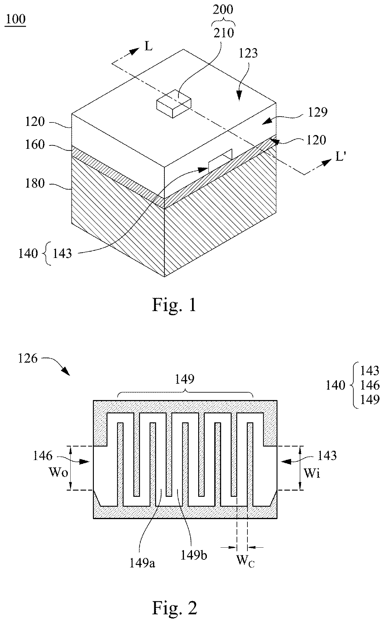
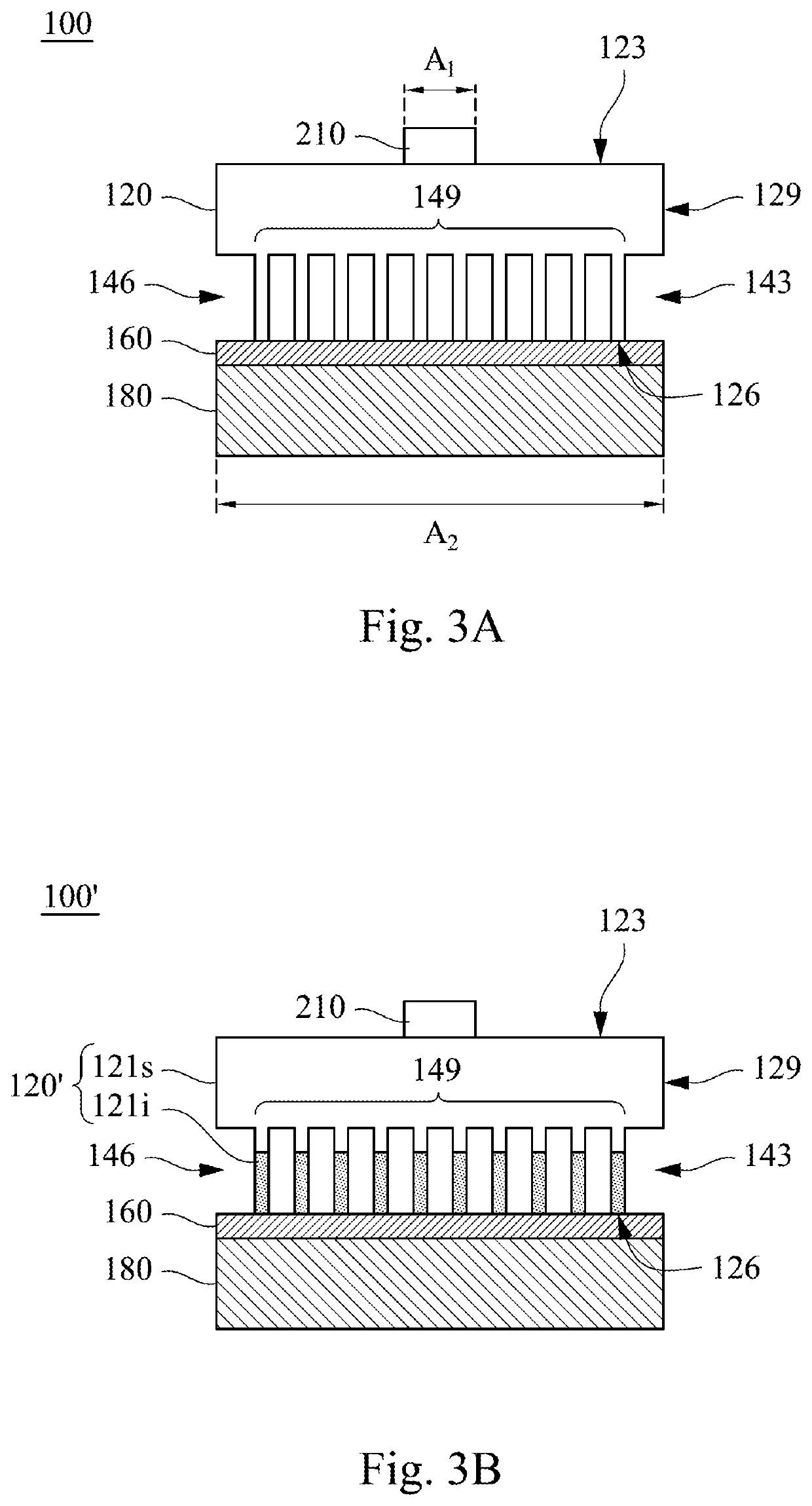
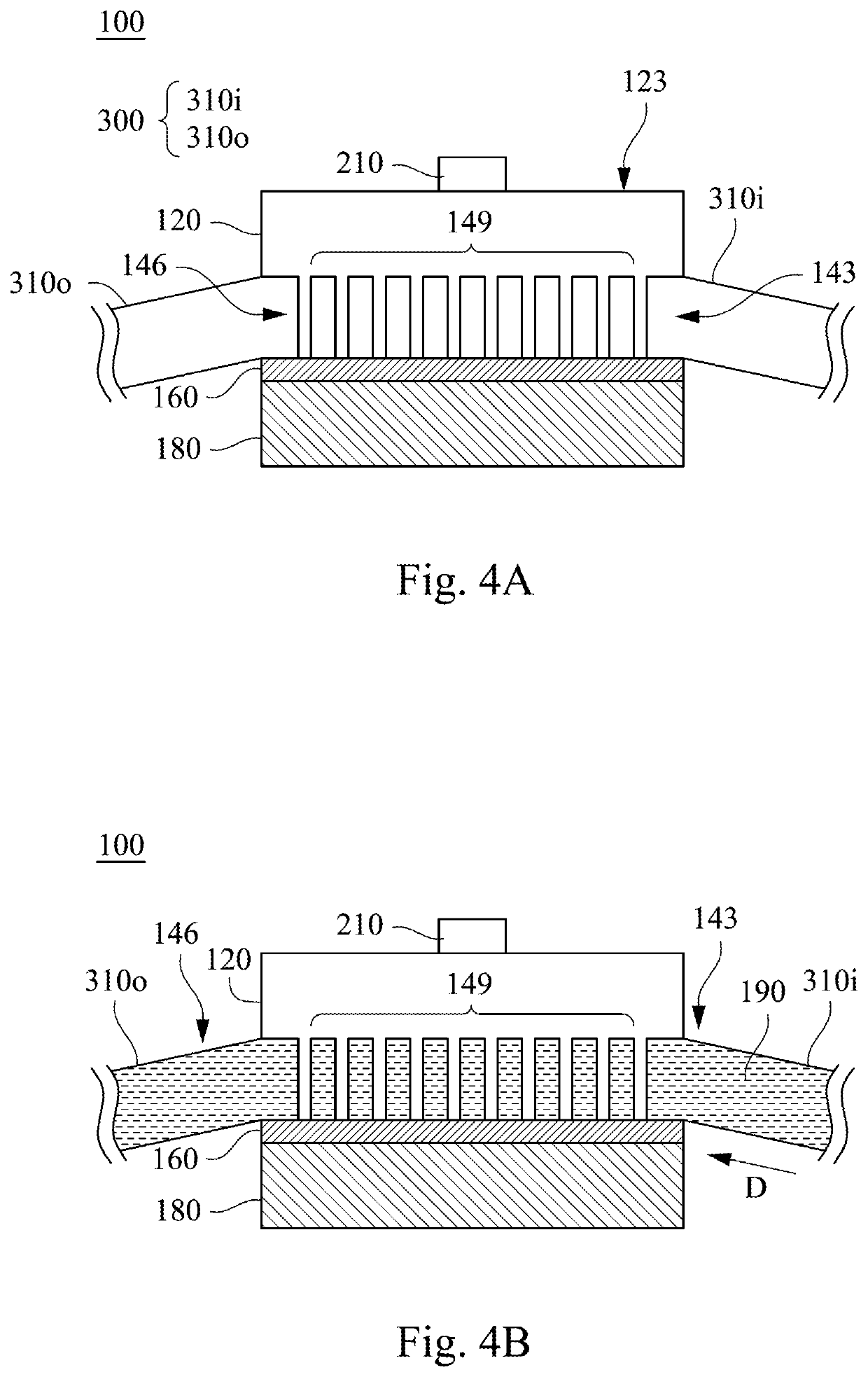
[0023]The following embodiments are disclosed with accompanying diagrams for detailed description. For illustration clarity, many details of practice are explained in the following descriptions. However, it should be understood that these details of practice do not intend to limit the present invention. That is, these details of practice are not necessary in parts of embodiments of the present invention. Furthermore, for simplifying the drawings, some of the conventional structures and elements are shown with schematic illustrations. Also, the same labels may be regarded as the corresponding components in the different drawings unless otherwise indicated. The drawings are drawn to clearly illustrate the connection between the various components in the embodiments, and are not intended to depict the actual sizes of the components.

[0024]As used herein, the terms “comprising,”“including,”“having,”“containing,”“involving,” and the like are to be understood to be open-ended, i.e., to mea...


PUM


Abstract

A thermal dissipation structure for integrated circuits includes a semiconductor substrate, a thermal dissipation trench, a metal seed layer and a metal layer. The semiconductor substrate has a first surface and a second surface which is opposite to the first surface. Integrated circuits are located on and thermally coupled with the first surface. The thermal dissipation trench is formed within the second surface. The metal seed layer seals the thermal dissipation trench to define a thermal dissipation channel. The thermal dissipation channel includes an inlet and an outlet. The metal layer is an electroplated layer formed from the metal seed layer.

Description

RELATED APPLICATIONS[0001]This application claims priority to Taiwan Application Serial Number 108124378, filed Jul. 10, 2019, which are herein incorporated by reference.BACKGROUNDField of Disclosure[0002]The present disclosure relates to a thermal dissipation structure for integrated circuits. More particularly, the present disclosure relates to the thermal dissipation of opto-electronic integrated circuits on the semiconductor substrate.Description of Related Art[0003]As the semiconductor industry moves to the limit of Moore's Law, conventional semiconductor integrated circuits encounter bottlenecks in development. In recent years, one of the solutions is Opto-electronic Integrated Circuit (OEIC), which integrates optical components and integrated circuits. For example, Silicon Photonics provides relatively low cost, while increasing transmission distance, reducing unit energy consumption, and increasing data bandwidth.[0004]Since a large number of optical components and integrate...

Claims


Application Information

Patent Timeline
IPC IPC(8): H01L23/46
CPCH01L23/46H01L21/4882H01L23/3672H01S5/02423
Inventor HORNG, RAY-HUAPAN, PO-CHOU
Owner NATIONAL CHIAO TUNG UNIVERSITY
Why Eureka
Try Eureka