Semiconductor device including ferroelectric material, neuromorphic circuit including the semiconductor device, and neuromorphic computing apparatus including the neuromorphic circuit

a technology of ferroelectric materials and semiconductor devices, applied in computing models, instruments, biological models, etc., can solve the problems of power consumption increase due to inefficient data transfer between main memory and computing apparatuses, and limitation of processing speed for calculating a large amount of data

Pending Publication Date: 2021-02-04
SAMSUNG ELECTRONICS CO LTD
View PDF3 Cites 2 Cited by
  • Summary
  • Abstract
  • Description
  • Claims
  • Application Information

AI Technical Summary

Benefits of technology

[0014]In some embodiments, a variation of a resistance of the third channel layer according to a signal applied to the gate electrode of the third transistor may have a symmetry.
[0015]In some embodiments, a resistance of the third channel layer according to a signal applied to the gate electrode of the third transistor may be linearly changed.

Problems solved by technology

In this way, a computing apparatus having a structure in which a main memory and an arithmetic logic device are separated generates a bottleneck phenomenon of data in a process of sequentially processing listed information and changing the information to a specific value in order to store the information in a desired and / or alternative predetermined memory device, and thus, the computing apparatus has a limitation in processing speed for calculating a large amounts of data.
Also, as a data capacity to be processed increases, power consumption increases due to inefficient data transfer between the main memory and the CPU.

Method used


Image

  • Semiconductor device including ferroelectric material, neuromorphic circuit including the semiconductor device, and neuromorphic computing apparatus including the neuromorphic circuit
  • Semiconductor device including ferroelectric material, neuromorphic circuit including the semiconductor device, and neuromorphic computing apparatus including the neuromorphic circuit
  • Semiconductor device including ferroelectric material, neuromorphic circuit including the semiconductor device, and neuromorphic computing apparatus including the neuromorphic circuit

Examples


Embodiment Construction

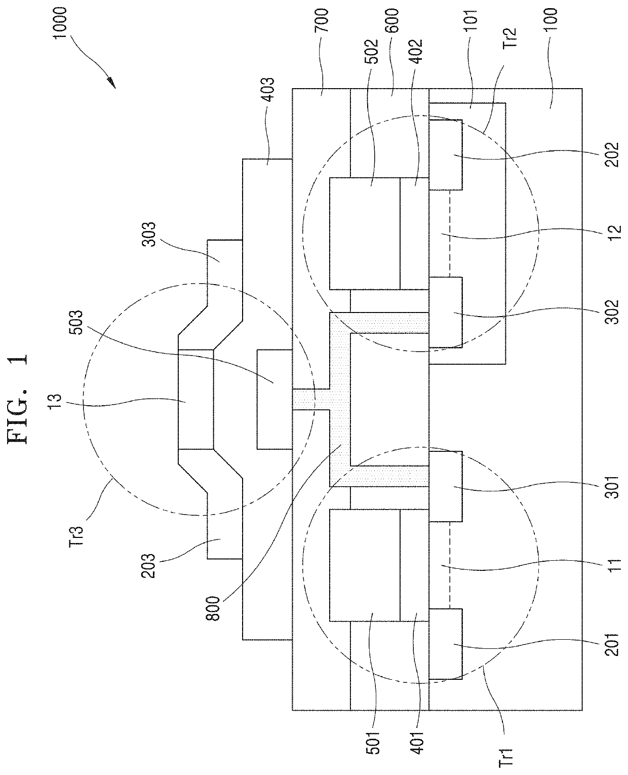
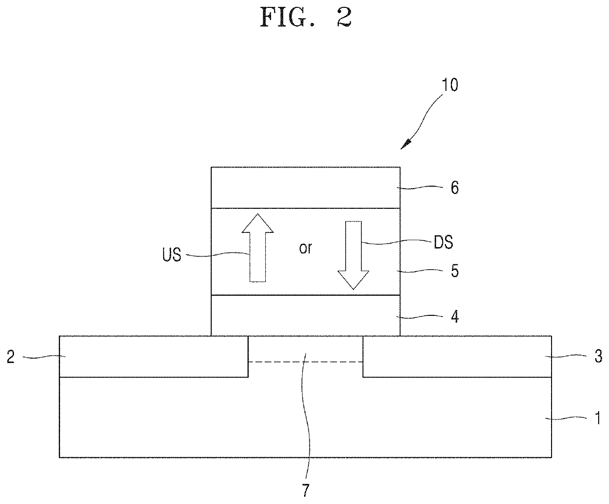
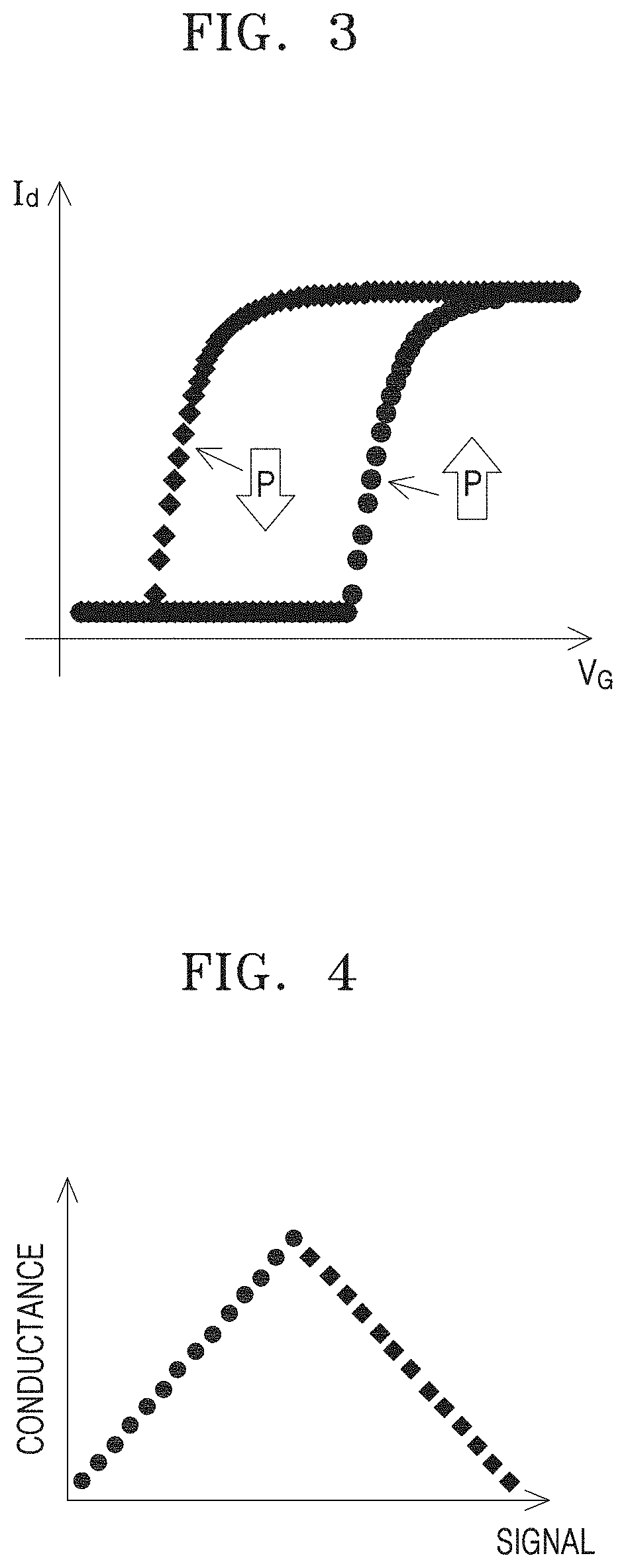
[0042]Reference will now be made in detail to embodiments, examples of which are illustrated in the accompanying drawings, wherein like reference numerals refer to like elements throughout. In this regard, inventive concepts may have different forms and should not be construed as being limited to the descriptions set forth herein. Accordingly, the embodiments are merely described below, by referring to the figures, to explain aspects. As used herein, the term “and / or” includes any and all combinations of one or more of the associated listed items. Expressions such as “at least one of” (e.g., at least one of A, B, and C), when preceding a list of elements, modify the entire list of elements and do not modify the individual elements of the list. For example, “at least one of A, B, and C,”“at least one of A, B, or C,”“one of A, B, C, or a combination thereof,” and “one of A, B, C, and a combination thereof,” respectively, may be construed as covering any one of the following combinatio...


PUM

PropertyMeasurementUnit
conductivityaaaaaaaaaa
thicknessaaaaaaaaaa
resistanceaaaaaaaaaa

Abstract

A semiconductor device includes a first transistor including a first channel layer of a first conductivity type, a second transistor provided in parallel with the first transistor and including a second channel layer of a second conductivity type, and a third transistor stacked on the first and second transistors. The third transistor may include a gate insulating film including a ferroelectric material. The third transistor may include third channel layer and a gate electrode that are spaced apart from each other in a thickness direction with the gate insulating film therebetween.

Description

CROSS-REFERENCE TO RELATED APPLICATION[0001]This application claims the benefit of Korean Patent Application No. 10-2019-0093357, filed on Jul. 31, 2019, in the Korean Intellectual Property Office, the disclosure of which is incorporated herein in its entirety by reference.BACKGROUND1. Field[0002]The present disclosure relates to semiconductor devices including a ferroelectric material, neuromorphic circuits including the semiconductor devices, and neuromorphic computing apparatuses including the neuromorphic circuits.2. Description of Related Art[0003]A computing apparatus of an existing Von Neumann Architecture has a structure including a cache memory for storing data, an arithmetic logic unit (ALU) for calculating data, and a controller for controlling these elements in a central processing unit (CPU) chip. Outside the CPU chip, a separate main memory (for example, DRAM) is provided, and data transfer between the main memory and the cache memory is performed through the controlle...

Claims


Application Information

Patent Timeline
Patent Type & Authority Applications(United States)
IPC IPC(8): H01L27/12G06N3/063G06N3/08
CPCH01L27/1207G06N3/08G06N3/063H01L27/0688H01L27/1225H01L27/0922H01L21/823857H01L21/8258G06N3/065H10B51/30H01L29/78391H01L29/40111H01L29/516H01L29/6684H01L21/823462H01L21/823412
Inventor KIM, SANGWOOKHEO, JINSEONGLEE, YUNSEONGJO, SANGHYUN
Owner SAMSUNG ELECTRONICS CO LTD
Why Eureka
Try Eureka