Semiconductor structure of work unit module

a work unit module and magnetic field technology, applied in the direction of semiconductor devices, semiconductor/solid-state device details, electrical apparatus, etc., can solve the problems of damage and affecting the normal work of the work unit, and achieve the effect of reducing the possibility of affecting the working chip and reducing the damage of external electromagnetic waves (e.g., noise)

Active Publication Date: 2021-02-18
GLOBAL UNICHIP CORPORATION +1
View PDF0 Cites 2 Cited by
  • Summary
  • Abstract
  • Description
  • Claims
  • Application Information

AI Technical Summary

Benefits of technology

[0006]Thus, through the construction of the embodiments above, when external electromagnetic waves (e.g., noises) pass through the encircling noise-resistance structure in a specific direction, since the impedance of the encircling noise-resistance structure is increased because of the arrangements of the first arrangement units and the second arrangement units, the damage of the external electromagnetic waves (e.g., noises) to the working chip is reduced so as to decrease the possibility of affecting the working chip in normal operation.

Problems solved by technology

However, since the arrangement characteristics of each of the noise isolation structures are too consistent to protect the entire range of the corresponding working unit so that external electromagnetic waves (e.g., noises) pass through one of sides of the noise isolation structure to reach the working unit in a specific direction, thereby damaging and affecting the normal work of the work unit.

Method used


Image

  • Semiconductor structure of work unit module
  • Semiconductor structure of work unit module
  • Semiconductor structure of work unit module

Examples


Embodiment Construction

[0015]Reference will now be made in detail to the present embodiments of the disclosure, examples of which are illustrated in the accompanying drawings. Wherever possible, the same reference numbers are used in the drawings and the description to refer to the same or like parts. According to the embodiments, it will be apparent to those skilled in the art that various modifications and variations can be made to the structure of the disclosure without departing from the scope or spirit of the disclosure.

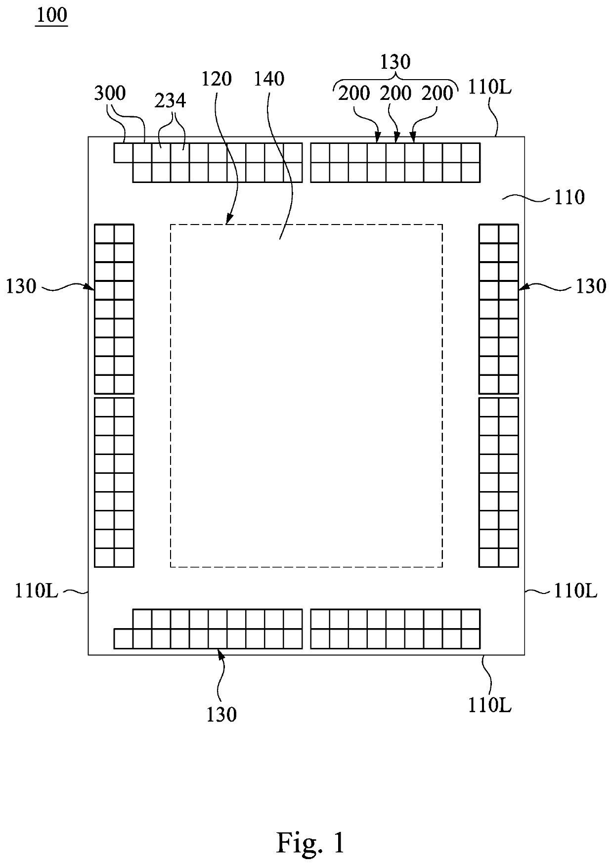
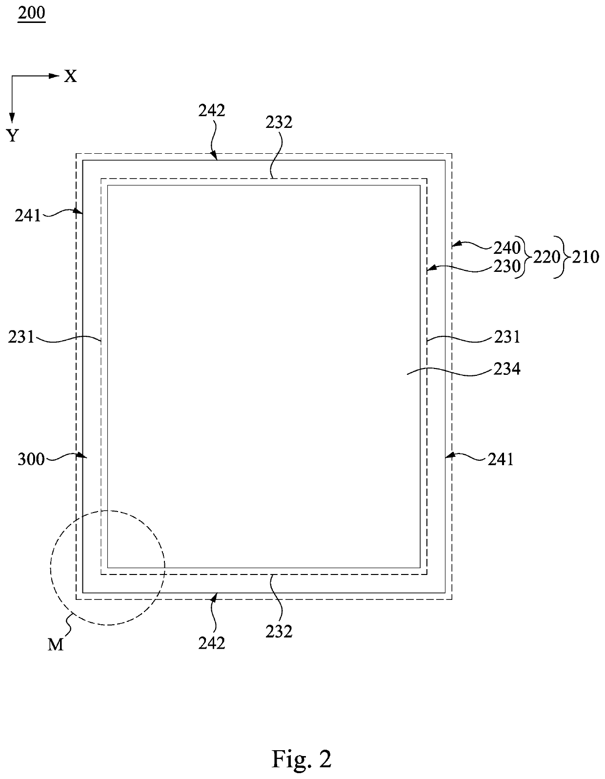
[0016]Reference is now made to FIG. 1, in which FIG. 1 is a layout arrangement view of a communication circuit module 100 according to one embodiment of the disclosure. As shown in FIG. 1, in this embodiment, a high speed communication product includes a configuration plane 110. The configuration plane 110 is defined with a central working area 120 and four chipsets 130. The central work area 120 is used to be mounted with a main chip 140 thereon. The chipsets 130 are respectively loc...


PUM

PropertyMeasurementUnit
semiconductoraaaaaaaaaa
noise-resistanceaaaaaaaaaa
noise-aaaaaaaaaa

Abstract

A semiconductor structure of a work unit module includes an encircling noise-resistance structure and a P-type substrate being defined with a chip region and a surrounding region surrounding the chip region. The surrounding area includes two first strip regions and two second strip regions. Each of the first strip regions is located between the second strip regions, and each of the second strip regions is located between the first strip regions. The encircling noise-resistance structure is located on the surrounding area, and includes first arrangement units and second arrangement units. The first arrangement unit is arranged in one of the first strip regions in a single row. The second arrangement unit is arranged in one of the second strip regions in a single row, and the long axis direction of the second arrangement unit is different from the long axis direction of the first arrangement unit.

Description

RELATED APPLICATIONS[0001]This application claims priority to Taiwan Application Serial Number 108128785, filed Aug. 13, 2019, which is herein incorporated by reference.BACKGROUNDField of Disclosure[0002]The disclosure relates to a semiconductor structure. More particularly, the disclosure relates to a semiconductor structure of a work unit module.Description of Related Art[0003]With the development of semiconductor technology, a conventional communication circuit module includes a main chip and a plurality of work units (e.g., serializer / deserializer, serdes). The main chip is surrounded by the work units. A noise isolation structure is placed to surround a periphery of each of the work units for isolating or at least reducing noise interference.[0004]However, since the arrangement characteristics of each of the noise isolation structures are too consistent to protect the entire range of the corresponding working unit so that external electromagnetic waves (e.g., noises) pass throu...

Claims


Application Information

Patent Timeline
Patent Type & Authority Applications(United States)
IPC IPC(8): H01L23/552H01L21/762
CPCH01L23/552H01L21/762H01L23/585H01L21/76224
Inventor TSENG, LI-YAYU, WEI-CHENGLI, BO-YANWANG, WEN-TAI
Owner GLOBAL UNICHIP CORPORATION
Why Eureka
Try Eureka