Printed circuit board and electronic device including same

a technology of printed circuit board and electronic device, which is applied in the association of printed circuit non-printed electric components, cross-talk/noise/interference reduction, and television systems, etc. it can solve the problems of difficult to arrange or provide signal lines, difficult to secure an area for further arranging signal lines, and difficult to miniaturize printed circuit boards. , to achieve the effect of avoiding electromagnetic interference and rapidly transmitting electric signals

Active Publication Date: 2021-03-04
SAMSUNG ELECTRONICS CO LTD
View PDF1 Cites 0 Cited by
  • Summary
  • Abstract
  • Description
  • Claims
  • Application Information

AI Technical Summary

Benefits of technology

[0009]Certain embodiments according to the present disclosure provide a printed circuit board capable of avoiding electromagnetic interference between signal lines while arranging the same number of signal lines in a smaller area and / or an electronic device including the same.
[0010]Certain embodiments according to this disclosure provide a printed circuit board capable of rapidly transmitting electric signals by selecting three signal lines from among the signal lines arranged in two adjacent wiring layers and an electronic device including the same.

Problems solved by technology

As the area for wiring the signal lines increases, it may be difficult to miniaturize the printed circuit board.
For example, although the signal quality and transmission speed are able to be improved by implementing a differential signal transmission method using two or more signal lines, since the size of a printed circuit board is limited in a miniaturized electronic device, for example, a mobile communication terminal, it may be difficult to arrange or provide the signal lines.
Although an additional area is required to add a plurality of signal lines, since the area of the printed circuit board is limited, it may be difficult to secure an area for further arranging the signal lines.

Method used


Image

  • Printed circuit board and electronic device including same
  • Printed circuit board and electronic device including same
  • Printed circuit board and electronic device including same

Examples


Embodiment Construction

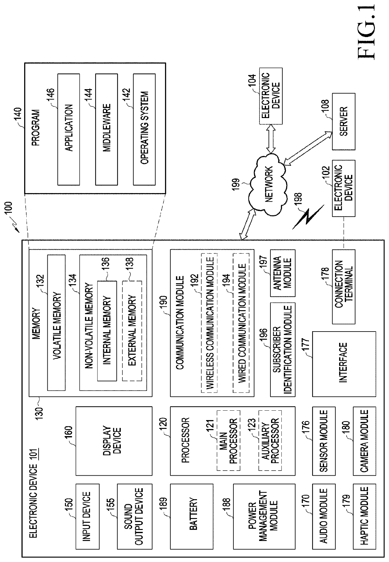
[0025]FIGS. 1 through 7, discussed below, and the various embodiments used to describe principles of the present disclosure in this patent document are by way of illustration only and should not be construed in any way to limit the scope of the disclosure. Those skilled in the art will understand that the principles of the present disclosure may be implemented in any suitably arranged system or device.

[0026]FIG. 1 is a block diagram illustrating an electronic device 101 in a network environment 100 according to various embodiments.

[0027]Referring to FIG. 1, the electronic device 101 in the network environment 100 may communicate with an electronic device 102 via a first network 198 (e.g., a short-range wireless communication network), or an electronic device 104 or a server 108 via a second network 199 (e.g., a long-range wireless communication network). According to an embodiment, the electronic device 101 may communicate with the electronic device 104 via the server 108. According...


PUM


Abstract

According to various embodiments, a printed circuit board may include: a first wiring layer including at least one first signal line and at least one first dummy line; and a second wiring layer arranged on the first wiring layer and including at least one second signal line and at least one second dummy line, wherein when the printed circuit board is viewed from above, the at least one first signal line may be arranged to overlap, at least in part, the at least one second dummy line, and the at least one second signal line may be arranged to overlap, at least in part, the at least one first dummy line.

Description

CROSS-REFERENCE TO RELATED APPLICATION[0001]This application is based on and claims priority under 35 U.S.C. § 119 to Korean Patent Application No. 10-2019-0106670 filed on Aug. 29, 2019 in the Korean Intellectual Property Office, the disclosure of which is incorporated by reference herein in its entirety.BACKGROUND1. Field[0002]Various embodiments disclosed in this document relate to a printed circuit board, for example, to a printed circuit board that transmits electric signals between electronic components using 3-phase interfaces and / or an electronic device including the same.2. Description of Related Art[0003]The development of electronic, information, and communication technologies has brought about integration of various functions into a single electronic device. For example, a smartphone includes functions, such as audio reproduction, photographing, or an electronic organizer, as well as functions for communication, and more various functions may be implemented in the smartp...

Claims


Application Information

Patent Timeline
Patent Type & Authority Applications(United States)
IPC IPC(8): H05K1/02H05K1/18H04N5/369
CPCH05K1/0245H05K1/028H05K1/181H05K1/0218H05K2201/10151H05K2201/09227H05K2201/093H05K2201/10121H05K2201/10128H04N5/369H05K2201/09781H05K1/0219H05K1/0298H05K2201/097H05K1/0246H04N25/70
Inventor HONG, EUNSEOKPARK, GYOUNGHWANCHUNG, CHEOLYOON
Owner SAMSUNG ELECTRONICS CO LTD
Why Eureka
Try Eureka