Organic electroluminescent element
a technology of electroluminescent elements and organic el elements, which is applied in the direction of luminescent compositions, organic chemistry, chemistry apparatus and processes, etc., can solve the problems of extending the life of phosphorescent organic el elements, requiring additional efficiency improvement, and reducing efficiency, so as to achieve stable skeleton, high level of control of charge injection/transport properties, and certain amount of injection and transport properties
- Summary
- Abstract
- Description
- Claims
- Application Information
AI Technical Summary
Benefits of technology
Problems solved by technology
Method used
Image
Examples
example 1
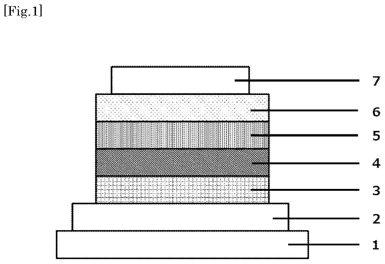
[0101]Each thin film was layered by vacuum vapor deposition at a vacuum of 4.0×10⁻⁵ Pa on a glass substrate on which an ITO anode had been formed in a film thickness of 110 nm. HAT-CN was first formed as a hole injection layer in a thickness of 25 nm on the ITO, followed by the formation of an NPD hole transport layer in a thickness of 30 nm. An HT-1 electron blocking layer was then formed in a thickness of 10 nm. The premix H1 as the host and Ir(ppy)3 as the light-emitting dopant were subsequently co-vapor deposited from different vapor deposition sources to form a light-emitting layer with a thickness of 40 nm. This co-vapor deposition was carried out under vapor deposition conditions that provided an Ir(ppy)3 concentration of 10 wt %. An ET-1 electron transport layer was then formed in a thickness of 20 nm. A 1 nm-thick lithium fluoride (LiF) electron injection layer was formed on the electron transport layer. Finally, a 70 nm-thick aluminum (Al) cathode was formed on the electro...
examples 2 to 9
[0102]Organic EL elements were fabricated proceeding as in Example 1, but respectively using each of the premixes H2 to H9 as the host in Example 1.
example 10
[0103]An organic EL element was fabricated proceeding as in Example 3, except that, after the formation of the light-emitting layer in Example 3, compound 1-11 was formed in a thickness of 10 nm as a hole blocking layer and ET-1 was formed in a thickness of 10 nm as an electron transport layer.
PUM
| Property | Measurement | Unit |
|---|---|---|
| weight loss temperatures | aaaaa | aaaaa |
| internal quantum efficiency | aaaaa | aaaaa |
| ionization potential | aaaaa | aaaaa |
Abstract
Description
Claims
Application Information


