Semiconductor light emitting device, exposure head, and image forming apparatus
- Summary
- Abstract
- Description
- Claims
- Application Information
AI Technical Summary
Benefits of technology
Problems solved by technology
Method used
Image

Examples
first embodiment
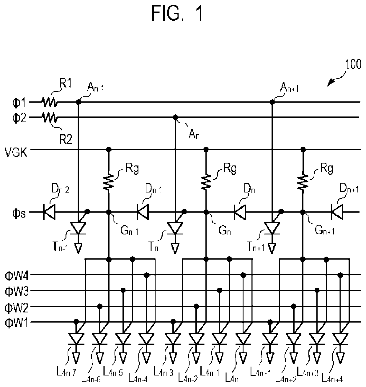
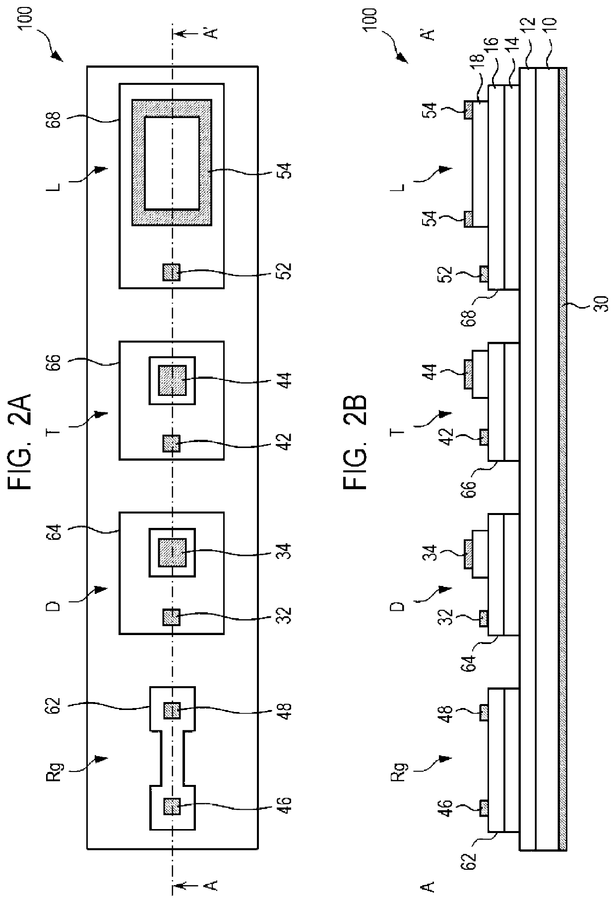
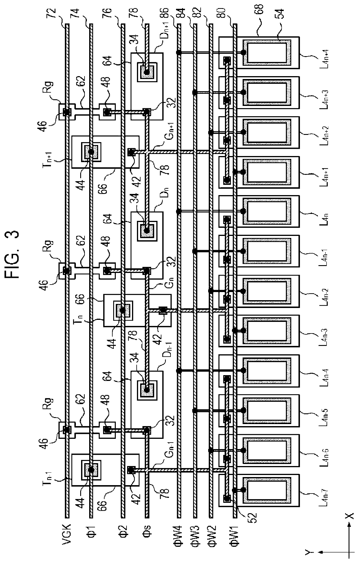
[0027]A schematic configuration of a semiconductor light emitting device according to a first embodiment of the present invention will be described with reference to FIG. 1 to FIG. 3. FIG. 1 is an equivalent circuit diagram for illustrating the schematic configuration of the semiconductor light emitting device according to the present embodiment. FIG. 2A and FIG. 2B are schematic views for illustrating basic structures of elements in the semiconductor light emitting device according to the present embodiment. FIG. 3 is a schematic view for illustrating an arrangement example of the elements in the semiconductor light emitting device according to the present embodiment.
[0028]As illustrated in FIG. 1, a semiconductor light emitting device 100 according to the present embodiment includes a plurality of shift thyristors T, a plurality of transfer diodes D, a plurality of light emitting thyristors L, input resistors R1 and R2, and a plurality of gate resistors Rg.
[0029]In the semiconduct...
second embodiment
[0102]A semiconductor light emitting device according to a second embodiment of the present invention will be described with reference to FIG. 11. The same components as those of the semiconductor light emitting device according to the first embodiment are denoted by the same reference symbols, and the description thereof is omitted or simplified. FIG. 11 is a schematic cross-sectional view for illustrating a structure of a shift thyristor in the semiconductor light emitting device according to the present embodiment.
[0103]In the first embodiment, the electrode 44 and the interconnection 94 (transfer signal line 74) are electrically connected to each other at three locations through the three opening portions 92B, 92A, and 92C arranged along the extending direction of the transfer signal line 74. However, the connection portion between the electrode 44 and the interconnection 94 may be provided to at least two locations on both sides of the mesa 66, and the number of connection port...
third embodiment
[0106]A semiconductor light emitting device according to a third embodiment of the present invention will be described with reference to FIG. 12. The same components as those of the semiconductor light emitting device according to the first and second embodiments are denoted by the same reference symbols, and the description thereof is omitted or simplified. FIG. 12 is a schematic cross-sectional view for illustrating a structure of a shift thyristor in the semiconductor light emitting device according to the present embodiment.
[0107]From the same viewpoint as that of the second embodiment, the semiconductor light emitting device according to the present embodiment is obtained by omitting the opening portion 92A formed in the upper surface of the mesa 66 from the semiconductor light emitting device according to the first embodiment. In a configuration of the present embodiment as well, the electrical connection between both sides of the mesa 66 can be maintained by the electrode 44,...
PUM
 Abstract
Description
Claims
Application Information
 - Generate Ideas
- Intellectual Property
- Life Sciences
- Materials
- Tech Scout
- Unparalleled Data Quality
- Higher Quality Content
- 60% Fewer Hallucinations
Browse by: Latest US Patents, China's latest patents, Technical Efficacy Thesaurus, Application Domain, Technology Topic, Popular Technical Reports.
© 2025 PatSnap. All rights reserved.Legal|Privacy policy|Modern Slavery Act Transparency Statement|Sitemap|About US| Contact US: help@patsnap.com