

Method for manufacturing high-sensitivity piezoresistive sensor using multi-level structure design
- Summary
- Abstract
- Description
- Claims
- Application Information
AI Technical Summary
Benefits of technology
Problems solved by technology
Method used
Image

Examples
embodiment 1
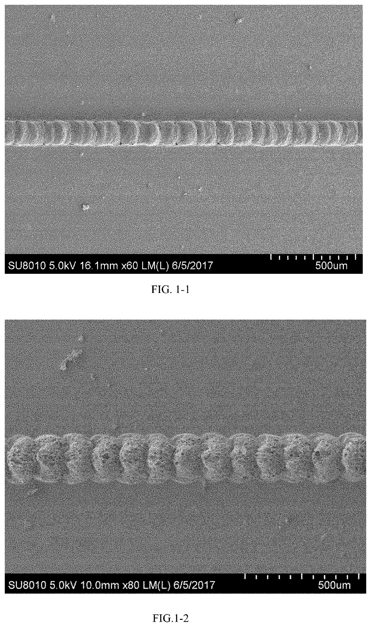
[0032] In a method for manufacturing a high-sensitivity piezoresistive sensor using a multi-level structure design, a method of multi-level contact design of the present invention is used to fabricate first a simplest contact form, which is linear patterns carbonized by laser with only stacking and contact between basic structural units.
[0033]A single dot obtained in a dotting mode is a basic geometrical unit formed by stacking basic structural units. Therefore, a dot line pattern has stacking of basic geometrical units and is a contact structure that is one level higher than a mere straight-line pattern. An overlapping portion between basic geometrical units undergoes laser energy twice, and therefore, basic structural units of the overlapping portion are weaker than those elsewhere, and come into contact or are disconnected more easily under the effect of an external force. Therefore, the sensitivity is high. A specific implementation is as follows:
[0034](1): A polyimide film purc...
embodiment 2
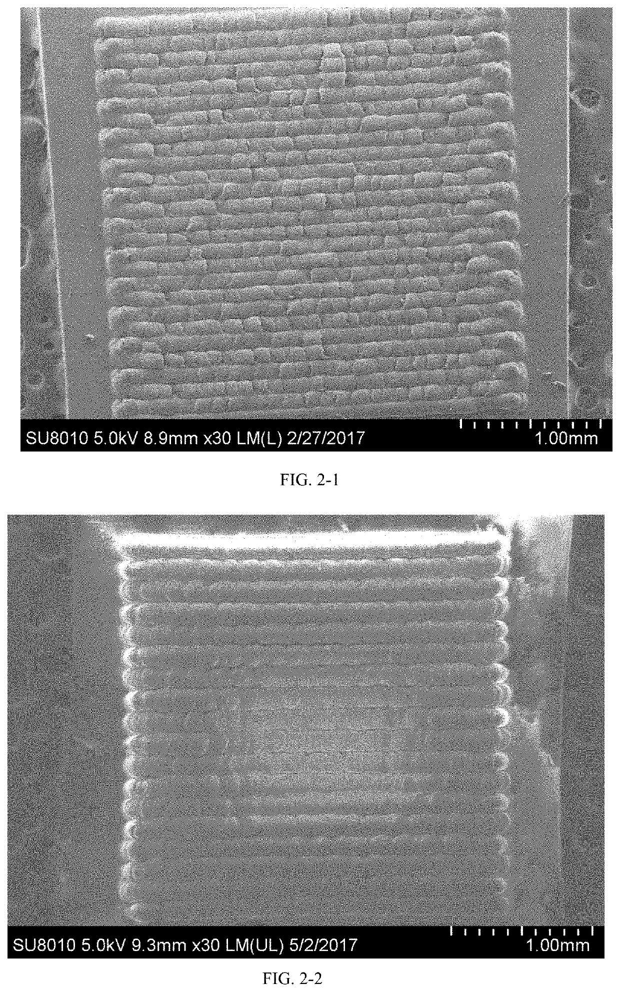
[0040] In a method for manufacturing a high-sensitivity piezoresistive sensor using a multi-level structure design, a structure in which basic structural units are stacked or contact is upgraded to a structure in which basic geometrical units are stacked. Next, a contact structure between the basic geometrical units may be designed. According to this method, when contact between basic geometrical units is weaker, the sensitivity is higher. In addition, a stacking status of basic structural units may be adjusted by changing laser energy. A specific implementation is as follows:
[0041](1): A polyimide film purchased from the DuPont Company is used, and the film has a thickness of 125 μm. A 30 mm*30 mm rectangle is drawn on laser operation software.
[0042](2): Laser parameters are set: A laser mode is a scan mode. A scan speed is 100 mm / s. A laser power is 37.5%. A scan interval is 150 mm.
[0043](3): A laser position is adjusted to perform in-situ carbonization on the film to generate a c...
embodiment 3
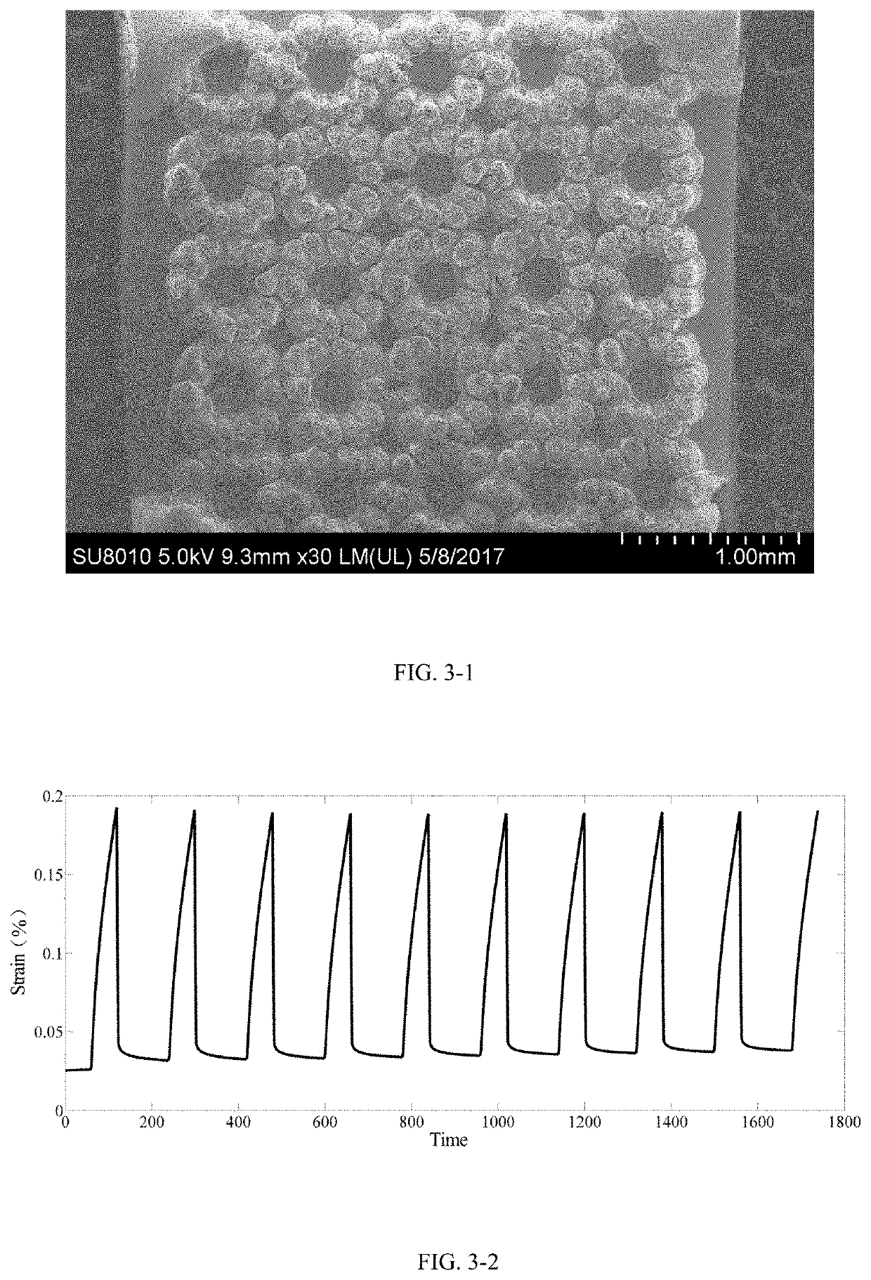
[0047] In a method for manufacturing a high-sensitivity piezoresistive sensor using a multi-level structure design, dot contact in the method is weaker than line contact. Therefore, a stacking structure of dot contact between basic geometrical structures is designed. A dot formed by stacking basic structural units is a first-level basic geometrical unit. A circle formed by arranging dot basic geometrical units is considered as a second-level basic geometrical unit. The second-level basic geometrical units are arranged in an array to form a surface, so as to form a surface-type pattern. In this pattern, first-level contact between basic geometrical units exists in the circle. Contact between circles is contact between the second-level basic geometrical units. Therefore, a multi-level contact structure is implemented. In this structure, dot contact makes contact portions relatively weak, and the contact portions are disconnected or come into contact easily under the influence of a str...
PUM
 Abstract
Description
Claims
Application Information