Non-volatile memory device and control method
- Summary
- Abstract
- Description
- Claims
- Application Information
AI Technical Summary
Benefits of technology
Problems solved by technology
Method used
Image
Examples
Embodiment Construction
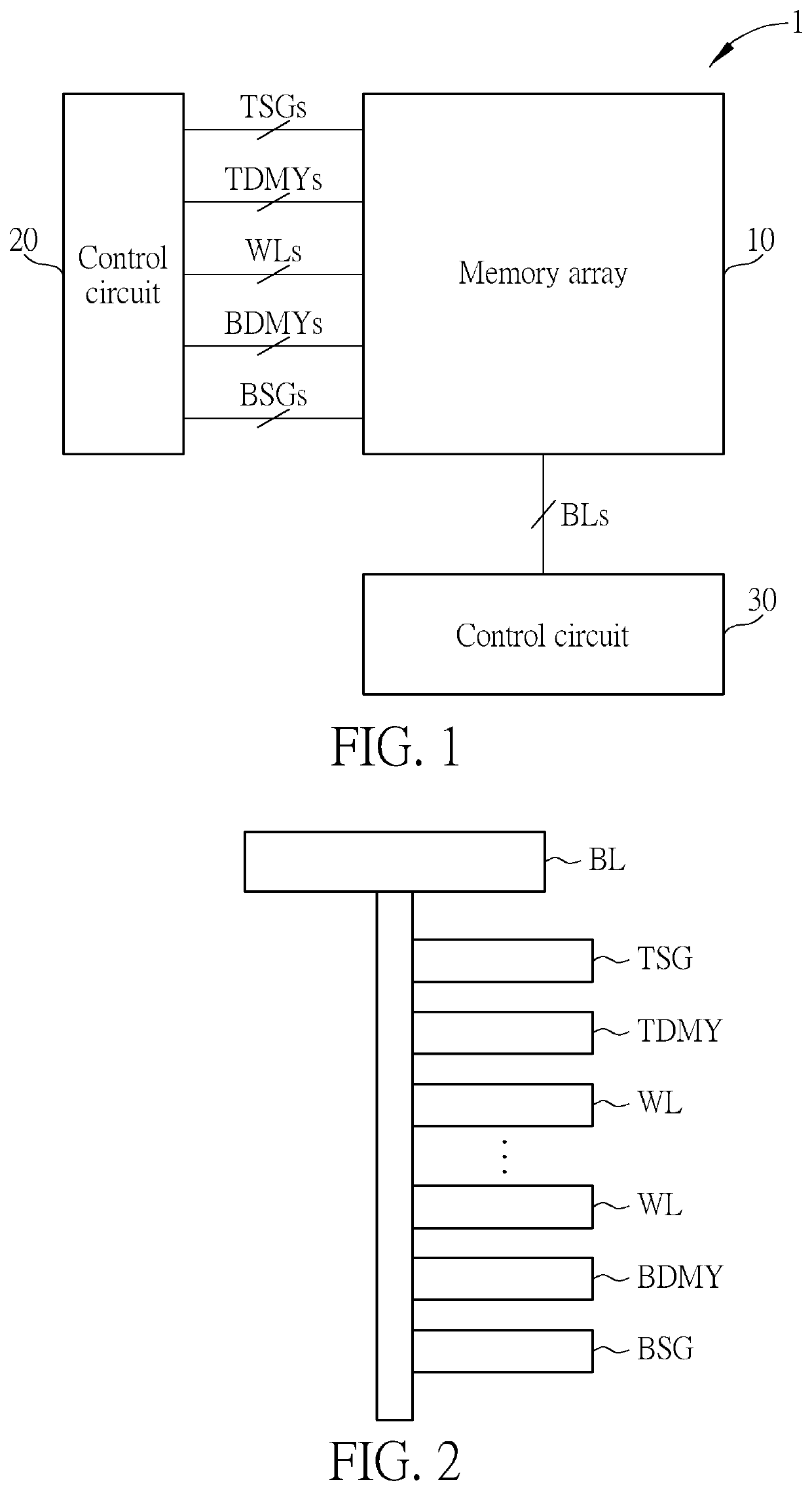
[0012]Please refer to FIG. 1, which is a schematic diagram of a non-volatile memory device 1 according to an embodiment of the present invention. The non-volatile memory device 1 may be an NAND flash memory.
[0013]For example, the non-volatile memory device 1 may be a three-dimensional (3D) NAND flash memory. The non-volatile memory device 1 includes a memory array 10 and control circuits 20 and 30. The memory array 10 includes a plurality of memory strings. Each memory string includes a plurality of memory cells. The memory cells of each string are connected together in series. The intersection of a word line and a semiconductor channel forms a memory cell. Top select gate lines TSGs, word lines WLs, top dummy word lines TDMYs, bottom dummy word lines BDMYs and bottom gate lines BSGs are connected between the memory array 10 and the control circuit 20. Bit lines BLs are connected between the memory array 10 and the control circuit 30.
[0014]FIG. 2 is a schematic diagram illustrating ...
PUM
 Abstract
Description
Claims
Application Information


