
Antenna device

Active Publication Date: 2021-04-29
MURATA MFG CO LTD
View PDF5 Cites 4 Cited by
  • Summary
  • Abstract
  • Description
  • Claims
  • Application Information

AI Technical Summary

Benefits of technology

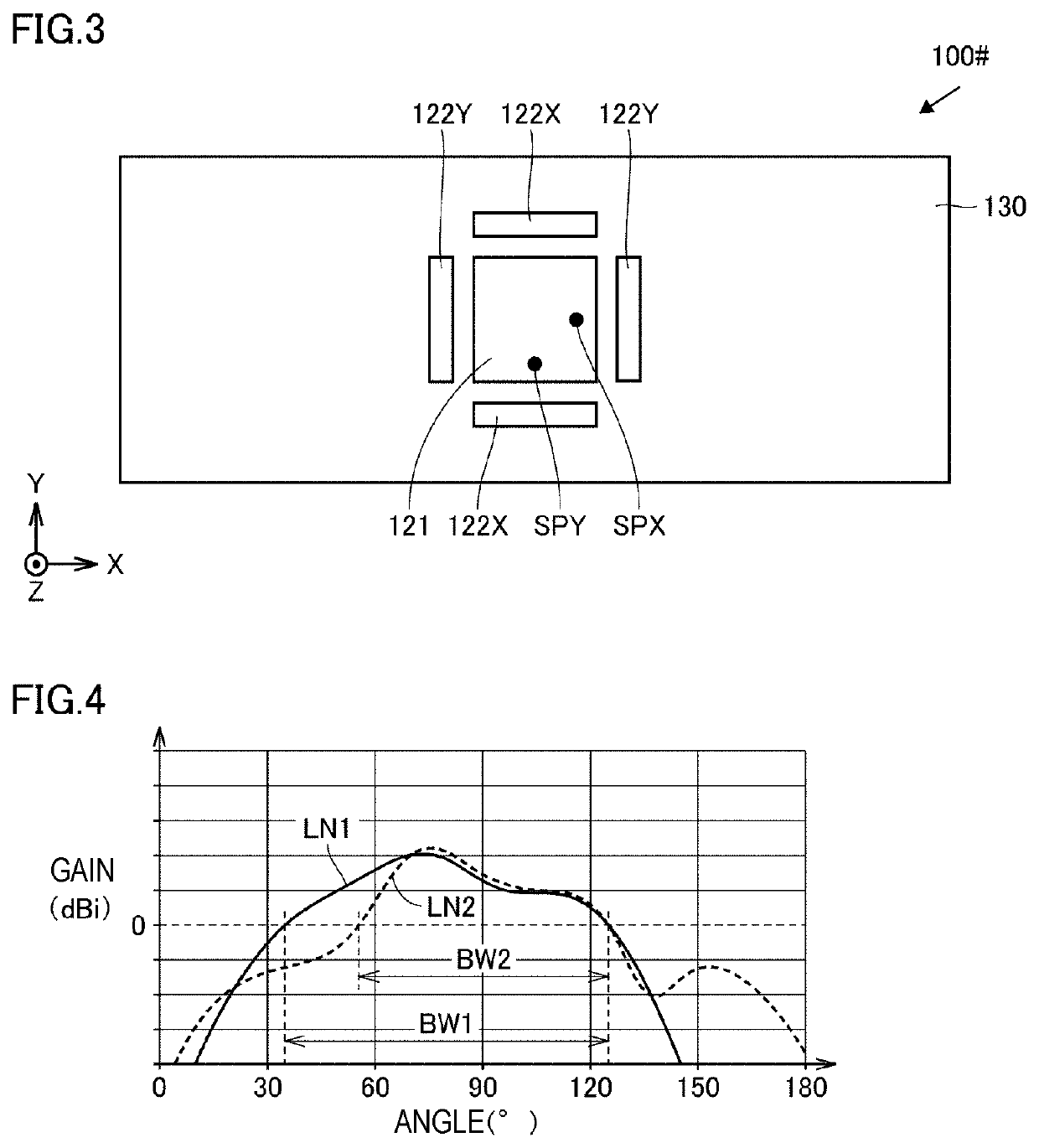
The present disclosure is about an antenna device that can radiate multiple polarized waves. The device has a parasitic element that improves the band width and expands the angle of the beam width. By using the parasitic element for one of the polarized waves, the device can suppress the narrowing of the beam width for the other wave while broadening its band width. This results in a balanced beam width and band width in the case of substrate size constraints. Overall, the device provides improved performance and flexibility in generating multiple polarized waves.

Problems solved by technology

However, in the case where a sufficient ground contact area cannot be secured with respect to the size of a radiating element (feed element+passive element) because of a constraint on the size of a dielectric substrate on or in which the feed element is arranged or any other similar constraint, the beam width of a radio wave radiated from an antenna becomes narrower compared with the case where the ground contact area is sufficiently large, and there may be a case where desired antenna characteristics cannot be obtained.

Method used


Image

  • Antenna device
  • Antenna device
  • Antenna device

Examples


embodiment 1

[0026](Basic Configuration of Communication Device)

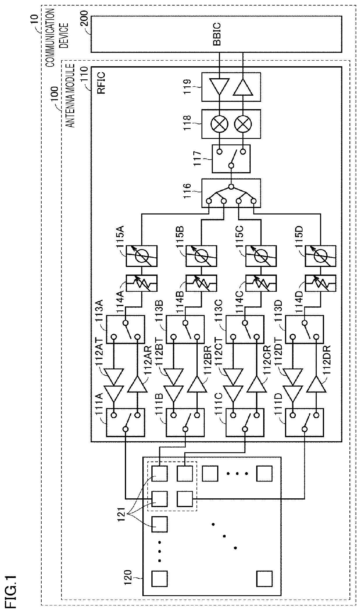
[0027]FIG. 1 is an example of a block diagram of a communication device 10 to which an antenna device 120 according to the embodiment 1 is applied. The communication device 10 is, for example, a mobile phone, a mobile terminal such as a smartphone, a tablet, or the like, a personal computer with a communication function, or the like.

[0028]Referring to FIG. 1, the communication device 10 includes an antenna module 100 and a BBIC 200 that makes up a baseband signal processing circuit. The antenna module 100 includes a RFIC 110 that is an example of a feed circuit and the antenna device 120. The communication device 10 up-converts a signal sent from the BBIC 200 to the antenna module 100 into a radio frequency signal and radiates the radio frequency signal from the antenna device 120, and down-converts a radio frequency signal received by the antenna device 120 and performs processing on the signal in the BBIC 200.

[0029]In FIG. 1, for ...

embodiment 2

[0055]In the embodiment 1, the example is described in which only one feed element is arranged in the antenna device.

[0056]In the embodiment 2, an example in which a plurality of feed elements is arranged in an array shape is described. In an array antenna, by adjusting the phases of radio frequency power supplied to adjacent feed elements, it becomes possible to use beamforming that changes the directivity (radiation angle) of a radio wave being radiated from the entire antenna.

[0057]FIG. 5 is a perspective view of an antenna device 120A according to the embodiment 2. Note that in FIG. 5, the RFIC 110 is not illustrated.

[0058]Referring to FIG. 5, in the antenna device 120A, four feed elements 121 are arranged on the dielectric substrate 130 in line along the X-axis direction. Furthermore, for each feed element 121, the parasitic elements 122X are formed at positions that face the sides of the feed element 121 parallel to the X-axis direction. Note that in the example of FIG. 5, the...

embodiment 3

[0064]In the embodiment 2, the example is described in which the dielectric substrate has a plane shape, and the array antenna radiates a radio wave in one direction.

[0065]In the embodiment 3, an example is described in which part of the dielectric substrate is bent, and the array antenna is capable of radiating a radio wave in different directions.

[0066]FIG. 10 is a perspective view of an antenna device 120C according to the embodiment 3. In the antenna device 120C, the dielectric substrate 130 includes a first part 135 parallel to the X-Y plane of FIG. 10 and a second part 136 that is bent from an end part of the first part 135 and parallel to the Z-X plane of FIG. 10. The length of a side of the first part 135 along the X-axis direction is La, and the length of a side of the first part 135 along the Y-axis direction is Lb. Furthermore, the length of a side of the second part 136 along the X-axis direction is also La, and the length of a side of the second part 136 along the Z-axi...


PUM


Abstract

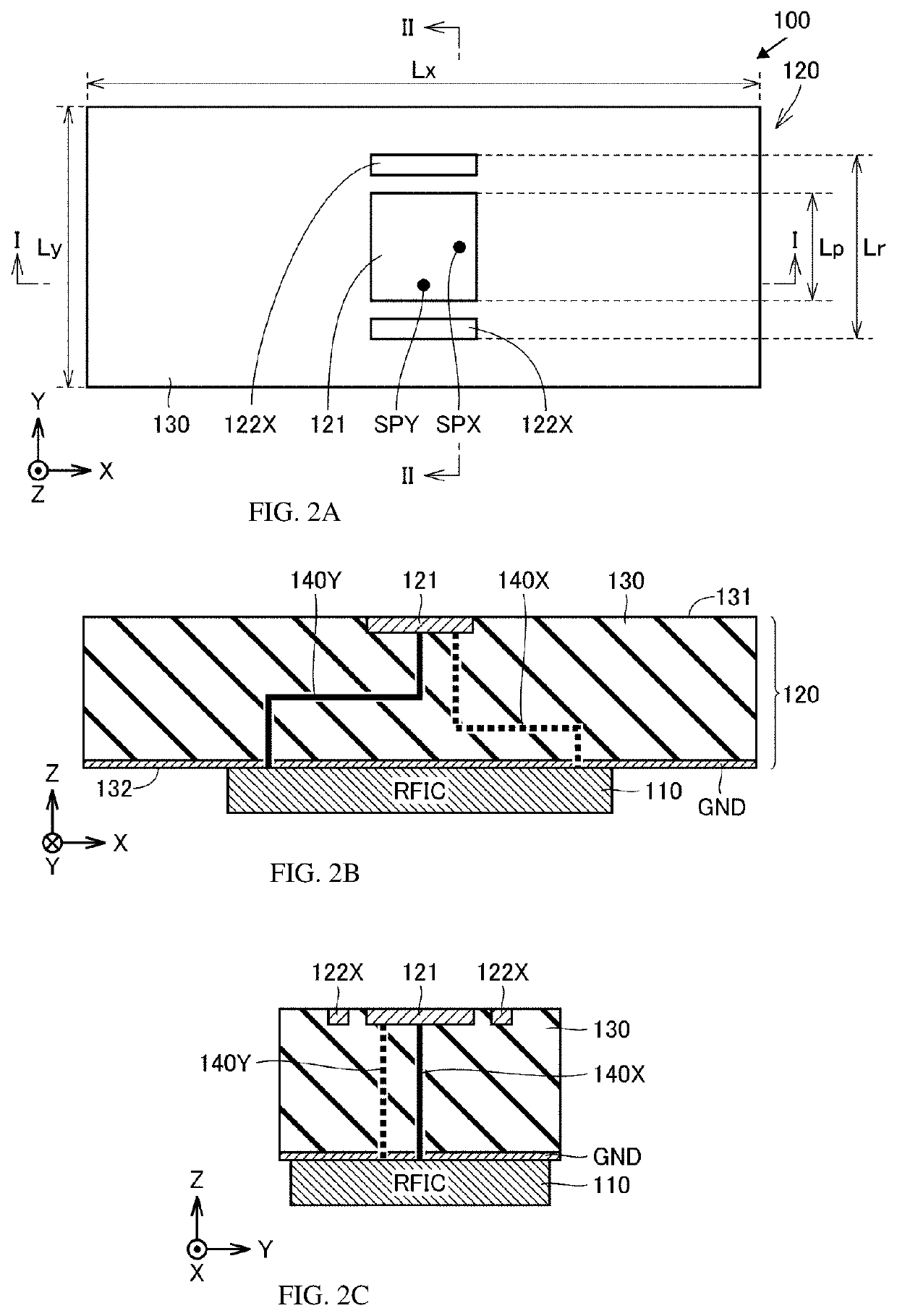
An antenna device includes a ground electrode, a feed element, and a parasitic element. The ground electrode has a substantially non-square rectangular plane shape that includes a first side extending in a first direction and a second side extending in a second direction orthogonal to the first direction. The feed element has a substantially rectangular plane shape and is formed in such a way that each side of the feed element becomes parallel to the first direction or the second direction. The parasitic element is formed in such a manner as to face a side of the feed element parallel to the first side. The feed element is configured to radiate a first polarized wave that excites in the first direction and a second polarized wave that excites in the second direction. The length of the first side is longer than the length of the second side.

Description

CROSS REFERENCE TO RELATED APPLICATION[0001]This is a continuation of International Application No. PCT / JP2019 / 029672 filed on Jul. 29, 2019 which claims priority from Japanese Patent Application No. 2018-145934 filed on Aug. 2, 2018. The contents of these applications are incorporated herein by reference in their entireties.BACKGROUND OF THE DISCLOSUREField of the Disclosure[0002]The present disclosure relates to antenna devices and more specifically to a technique that improves characteristics of an antenna device with parasitic elements.Description of the Related Art[0003]In flat plate shape patch antennas, a configuration that adjusts antenna characteristics by arranging passive elements (parasitic elements) around a feed element is known.[0004]Japanese Unexamined Patent Application Publication No. 2008-312263 (Patent Document 1) discloses, in a microstrip antenna having a flat plate shape, a configuration in which a plurality of passive elements are arranged around a feed eleme...

Claims


Application Information

Patent Timeline
IPC IPC(8): H01Q5/35H01Q5/378H01Q1/22H01Q5/28H01Q9/04
CPCH01Q5/35H01Q5/378H01Q9/0414H01Q5/28H01Q1/2208H01Q21/065H01Q21/08H01Q3/30H01Q19/005H01Q21/24H01Q1/48H01Q9/045
Inventor SUDO, KAORUONAKA, KENGO
Owner MURATA MFG CO LTD
Learn More